Microarchitecture: Out-Of-Order execution(OoOE/OOE) & Register Renaming

乱序执行的步骤

简单来说每个阶段执行的操作如下:^1

1)获取指令,解码后存放到执行缓冲区Reservations Stations
2)乱序执行指令,结果保存在一个结果序列中
3)退休期Retired Circle,重新排列结果序列及安全检查(如地址访问的权限检查),提交结果到寄存器

  1. 取指令/uops
  2. 指令(uops)dispatch 到instruction queue (/instruction buffer / reservation stations).
  3. 指令等待操作数指令可用,然后可以在前后指令前离开等待队列
  4. issue到对应port单元执行,并且在 scheduler(reservation station)里跟踪uops依赖。
  5. 结果缓存在(re-order buffer, ROB)
    1. 在Tomasulo算法中,重排序缓冲区(英语:re-order buffer, ROB))可以使指令在乱序执行,之后按照原有顺序提交。
  6. 按照程序序结束(只有前面的指令都完成写回寄存器的操作),该指令才能retire
    1. 在retire的时候,重新排序运算结果来实现指令的顺序执行中的运行结果

why out-of-order execution retire/commit in program order

  1. 对于程序员外部视角来看,程序还是按序执行的。
  2. 如果指令出错,可以精确定位exceptions 位置,并且执行回滚来复原。
  3. ???寄存器数据依赖(重命名打破?)

乱序执行的实现

scoreboard

只有当一条指令与之前已发射(issue)的指令之间的冲突消失之后,这条指令才会被发射、执行。

如果某条指令由于数据冲突而停顿,计分板会监视正在执行的指令流,在所有数据相关性造成的冲突化解之后通知停顿的指令开始执行。

Tomasulo 托马苏洛算法

通过寄存器重命名机制,来解决后两种数据依赖。

使用了共享数据总线(common data bus, CDB)将已计算出的值广播给所有需要这个值作为指令源操作数的保留站

在指令的发射(issue)阶段,如果操作数和保留站都准备就绪,那么指令就可以直接发射并执行。

如果操作数未就绪,则进入保留站的指令会跟踪即将产生这个所需操作数的那个功能单元。

乱序执行的发展

随着流水线pipeline的加深和主存(或者缓存)和处理器间的速度差的变大。在顺序执行处理器等待数据的过程中,乱序执行处理器能够执行大量的指令。使得乱序执行更加重要。

Register Renaming

来由

已知可以通过乱序执行来实现,硬件资源的高效利用(避免计算指令等待访存指令的完成)。为了实现乱序执行,需要通过寄存器重命名来打破寄存器的之间的读写依赖。

例子1

对于原始代码

1
2
3
4
5
6
1. R1=M[1024]
2. R1=R1+2
3. M[1032]=R1
4. R1=M[2048]
5. R1=R1+4
6. M[2056]=R1

原本代码前后3条是没有关系的,可以并行的。需要使用寄存器重命名来解决R1的读后写依赖。

1
2
3
1. R1=M[1024] 4. R2=M[2048]
2. R1=R1+2 5. R2=R2+4
3. M[1032]=R1 6. M[2056]=R2

数据冲突

如果多条指令使用了同一个存储位置,这些指令如果不按程序地址顺序执行可能会导致3种数据冲突(data hazard):

  • 先写后Read-after-write,RAW):从寄存器或者内存中读取的数据,必然是之前的指令存入此处的。直接数据相关(true data dependency)

  • 先写后Write-after-write,WAW):连续写入特定的寄存器或内存,那么该存储位置最终只包含第二次写的数据。这可以取消或者废除第一次写入操作。WAW相关也被说成是“输出相关”(output dependencies)。

  • 先读后Write-after-read,WAR):读操作获得的数据是此前写入的,而不是此后写操作的结果。因此并行和乱序时无法改善的资源冲突(antidependency)。

后面两个WAW和WAR可以通过寄存器重命名解决(register renaming),不必等待前面的读写操作完成后再执行写操作,可以保持这个存储位置的两份副本:老值与新值。

前一条指令的读老值的操作可以继续进行,无需考虑那些后一条指令的写新值甚至该写新值指令之后的读新值的操作。产生了额外的乱序执行机会。当所有读老值操作被满足后,老值所使用的寄存器既可以释放。这是寄存器重命名的实质

重命名存储对象

任何被读或写的存储都是可以被重名。

  1. 最常考虑的是通用整数寄存器与浮点寄存器。
  2. 标志寄存器、状态寄存器甚至单个状态位也是常见的重命名的对象。
  3. 内存位置也可以被重命名,虽然这么做不太常见。

通用(逻辑)寄存器和物理寄存器

对于某种ISA,有固定的供编译器/汇编器访问使用的寄存器。例如,Alpha ISA使用32个64位宽整数寄存器,32个64位宽浮点寄存器。

但是一款特定的处理器,实现了这种处理器体系结构。例如Alpha 21264有80个整数寄存器、72个浮点寄存器,作为处理器内物理实现的寄存器。

寄存器个数设计考虑

如果寄存器个数很多,就不需要寄存器重命名机制。比如IA-64指令集体系结构提供了128个通用寄存器。但是这会导致一些问题:

  1. 编译器如果需要重用寄存器会很容易导致程序尺寸大增
    1. 程序的循环连续迭代执行就需要复制循环体的代码以使用不同的寄存器,这种技术叫做循环展开。
    2. 代码尺寸增加,会导致指令高速缓存的未命中(cache miss)增加,处理器执行停顿等待从低级存储中读入代码。这对运算性能的影响是致命的。
  2. 大量的寄存器,需要在指令的操作数中需要很多位表示,导致程序尺寸变大。
  3. 很多指令集在历史上就使用了很少的寄存器,出于兼容原因现在也很难改变。

实现方法简述

  1. tag索引的寄存器堆(tag-indexed register file)
  2. 保留站(reservation station)方法
    1. 通常是每个执行单元的输入口都有一个物理寄存器堆

相关寄存器部件

  1. 远期寄存器堆(Future File):
    1. 处理器对分支做投机执行的寄存器的状态保存于此。
    2. 使用逻辑寄存器号来索引访问。
  2. 历史缓冲区(History Buffer):
    1. 用于保存分支时的逻辑寄存器状态。
    2. 如果分支预测失败,将使用历史缓冲区的数据来恢复执行状态。
  3. 排缓冲区(Reorder Buffer,ROB):
    1. 为了实现指令的顺序提交,处理器内部使用了一个Buffer。如果在该缓冲区中排在一条指令之前的所有都已经提交,没有处于未提交状态的(称作in flight),则该指令也被提交(即确认执行完毕)。
    2. 因此重排缓冲区是在远期寄存器堆之后,体系结构寄存器堆之前。提交的指令的结果写入体系寄存器堆。
  4. 体系结构寄存器堆(Architectural Register File)或者引退寄存器堆(Retirement Register File,RRF):
    1. 存储了被提交的体系寄存器的状态。通过逻辑寄存器的号来查询这个寄存器堆。
    2. 重排序缓冲区(reorder buffer)中的引退(retired)或者说提交(committed)指令,把结果写入这个寄存器堆。

所属部件

  1. 编译器
    1. 会尽力检测出类似这样的问题,并把不同的寄存器分配给不同的指令使用。但是,受指令集体系结构的限制,汇编程序可以使用的寄存器名字的数量是有限的。
  2. 硬件实现
    1. 在处理器指令流水线执行时把这些指令集体系结构寄存器映射为不同的物理寄存器。
    2. 比如下图的Renamer / Allocator(也称为Resource Allocation Table (RAT))将架构寄存器映射到物理寄存器。 它还为loads and stores分配资源,并将uops分到不同端口。

需要进一步的研究学习

暂无

遇到的问题

暂无

开题缘由、总结、反思、吐槽~~

参考文献

https://zh.wikipedia.org/zh-cn/%E4%B9%B1%E5%BA%8F%E6%89%A7%E8%A1%8C

https://easyperf.net/blog/2018/04/22/What-optimizations-you-can-expect-from-CPU

Microarchitecture: Pipeline of Intel Core CPUs

skyLake in wikichip

简化图 in uiCA

名称解释

  1. Scheduler
    1. address-generation unit (AGU),

多端口发射模型

每个端口的函数可能一个周期执行不完。但是是形成了流水线的。可以保证每个周期accept一个新uops

需要进一步的研究学习

暂无

遇到的问题

暂无

开题缘由、总结、反思、吐槽~~

参考文献

Microarchitecture: Zero (one) idioms & Mov Elimination

微架构的关系

寄存器重命名是乱序执行Tomasulo算法的一部分

寄存器重命名可以实现:

  1. 部分mov消除
  2. NOPs
  3. zero (one) idioms
    对于这些指令,无序发射到scheduler。可以直接在reorder buffer写入结果。

Zero (one) idioms

Zero (one) idioms 是不管原寄存器src值是什么,结果/目的寄存器dst一直/一定是0 (1)的一类指令。比如:XOR一个寄存器和自己。

  1. 由于是在寄存器重命名阶段(Rename)时实现的
    1. 所以不需要发射到port执行单元执行,占用硬件资源。也没有延迟
    2. 但是需要划分前面部分的decode的带宽,和ROB(reorder buffer)的资源
      1
      2
      sub eax, eax
      xor eax, eax

例子

使用uarch-bench

1
2
3
xor eax, eax
dec edi
jnz .loop

由于第一条指令是Zero idioms;后两条指令可以macro-fusion。

所以各部分平均执行次数为

指令个数 UOPS_ISSUED UOPS_EXECUTED UOPS_RETIRED
3 2 1 2

特殊的情况

有些架构可能不支持srcImm0-dstReg的指令的Zero idioms

1
mov eax, 0 

mov Elimination

  1. 由于是在寄存器重命名阶段(Rename)时实现的
    1. 所以不需要发射到port执行单元执行,占用硬件资源。也没有延迟
    2. 但是需要划分前面部分的decode的带宽,和ROB(reorder buffer)的资源

例子

1
2
3
4
5
add eax,4
mov ebx,eax ; //寄存器重命名,ebx指向eax即可
sub ebx,ecx
dec edi
jnz .loop

由于第二条指令是mov Elimination;后两条指令可以macro-fusion。

所以各部分平均执行次数为

指令个数 UOPS_ISSUED UOPS_EXECUTED UOPS_RETIRED
5 4 3 4

被覆盖的结果是否能消除

1
2
3
4
mov eax, 1 ; will be eliminated?
mov eax, 2
dec edi
jnz .loop

第一个mov被覆盖了。这是属于编译器的工作。CPU做不到这点(即使做得到,为了实现这点设计的硬件开销也会很大,不值得)

无效操作是否能消除

一般和0的立即数作用有关

1
2
xor eax, eax 
sub ebx, eax ; will be eliminated? (eax is always 0)

第二条指令在IvyBridge也不会消除。这同样是编译器的工作

但是llvm-mca通过ZeroRegister的实现,可以消除。

类似的还有

1
2
3
mov eax, 0
mov ebx, 0
cmp eax, ebx ; eax and ebx are always equal

一般也不会消除。这同样是编译器的工作

需要进一步的研究学习

暂无

遇到的问题

暂无

开题缘由、总结、反思、吐槽~~

参考文献

https://randomascii.wordpress.com/2012/12/29/the-surprising-subtleties-of-zeroing-a-register/

https://easyperf.net/blog/2018/04/22/What-optimizations-you-can-expect-from-CPU

https://zh.m.wikipedia.org/zh-hans/%E5%AF%84%E5%AD%98%E5%99%A8%E9%87%8D%E5%91%BD%E5%90%8D

cuda Assembly:PTX & SASS

两种汇编

  1. parallel thread execution (PTX) 内联汇编有没有关系
    1. PTX是编程人员可以操作的最底层汇编,原因是SASS代码的实现会经常根据GPU架构而经常变换
    2. https://docs.nvidia.com/cuda//pdf/Inline_PTX_Assembly.pdf
    3. ISA指令手册 https://docs.nvidia.com/cuda/parallel-thread-execution/index.html#instruction-set
  2. SASS
    1. Streaming ASSembly(Shader Assembly?) 没有官方的证明
    2. 没有官方详细的手册,有基本介绍:https://docs.nvidia.com/cuda/cuda-binary-utilities/index.html#ampere
    3. https://zhuanlan.zhihu.com/p/161624982
    4. 从可执行程序反汇编SASS
      1. https://www.findhao.net/easycoding/2339.html

SASS 指令基本信息

对于Ampere架构

指令方向

1
(instruction) (destination) (source1), (source2) ...

各种寄存器说明

  • RX for registers
  • URX for uniform registers
  • SRX for special system-controlled registers
  • PX for predicate registers
  • c[X][Y] for constant memory

SASS 举例说明1

SASS的难点在于指令的后缀。由于手册确实,需要结合PTX的后缀查看

1
2
3
/*0028*/         IMAD R6.CC, R3, R5, c[0x0][0x20]; 
/*0030*/ IMAD.HI.X R7, R3, R5, c[0x0][0x24];
/*0040*/ LD.E R2, [R6]; //load

line1

1
/*0028*/ IMAD R6.CC, R3, R5, c[0x0][0x20];

Extended-precision integer multiply-add: multiply R3 with R5, sum with constant in bank 0, offset 0x20, store in R6 with carry-out.

c[BANK][ADDR] is a constant memory。

.CC means “set the flags”

line2

1
/*0030*/ IMAD.HI.X R7, R3, R5, c[0x0][0x24];

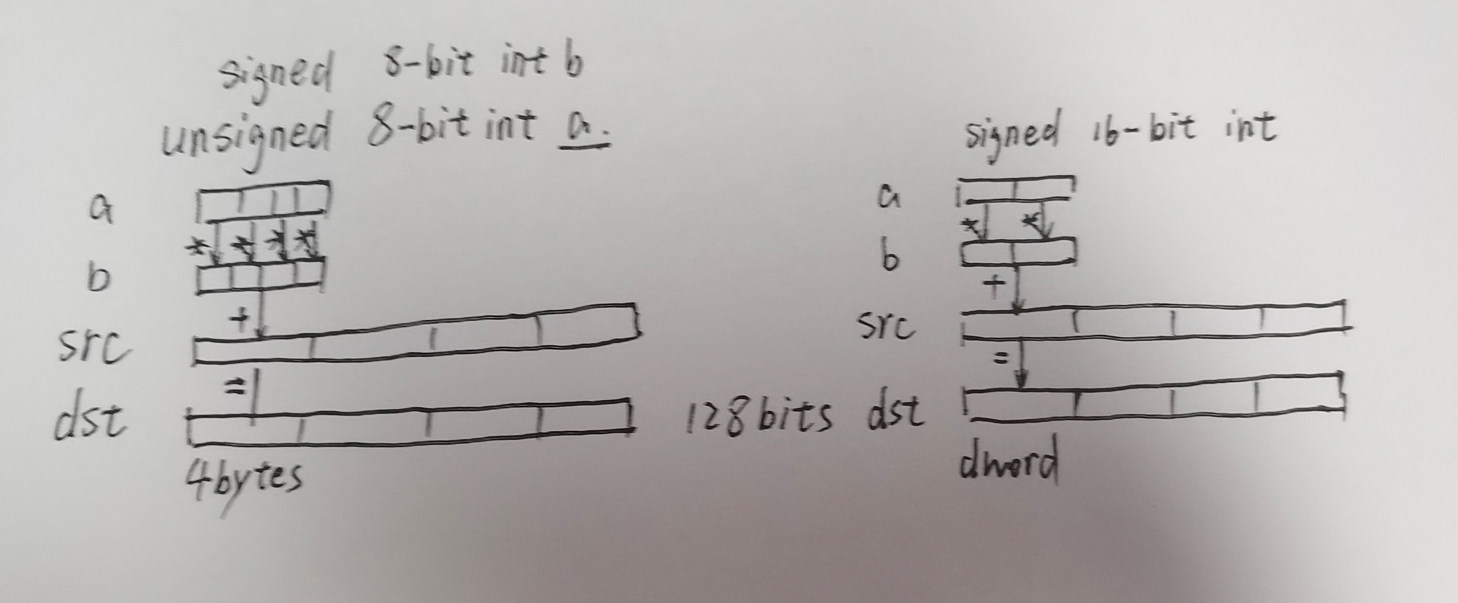
Integer multiply-add with extract: multiply R3 with R5, extract upper half, sum that upper half with constant in bank 0, offset 0x24, store in R7 with carry-in.

line3

1
/*0040*/         LD.E R2, [R6]; //load

LD.E is a load from global memory using 64-bit address in R6,R7(表面上是R6,其实是R6 与 R7 组成的地址对)

summary

1
2
3
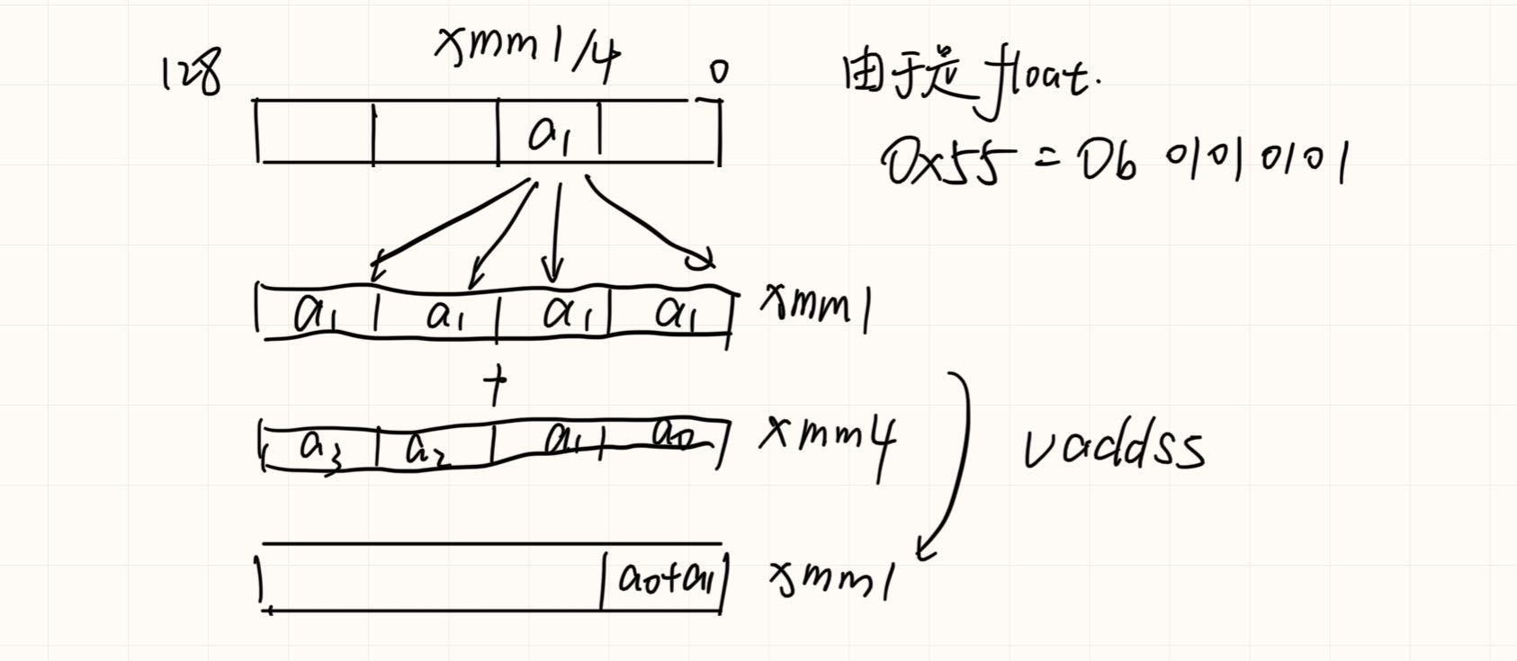
R6 = R3*R5 + c[0x0][0x20], saving carry to CC
R7 = (R3*R5 + c[0x0][0x24])>>32 + CC
R2 = *(R7<<32 + R6)

寄存器是32位的原因是 SMEM的bank是4字节的。c数组将32位的基地址分开存了。

first two commands multiply two 32-bit values (R3 and R5) and add 64-bit value c[0x0][0x24]<<32+c[0x0][0x20],

leaving 64-bit address result in the R6,R7 pair

对应的代码是

1
2
3
4
kernel f (uint32* x) // 64-bit pointer
{
R2 = x[R3*R5]
}

SASS Opt Code分析2

  • LDG - Load form Global Memory
  • ULDC - Load from Constant Memory into Uniform register
  • USHF - Uniform Funnel Shift (猜测是特殊的加速shift)
  • STS - Store within Local or Shared Window

流水STS

观察 偏移

  • 4
  • 2060(delta=2056)
  • 4116(delta=2056)
  • 8228(delta=2 * 2056)
  • 6172(delta=-1 * 2056)
  • 10284(delta=2 * 2056)
  • 12340(delta=2056)

可见汇编就是中间写反了,导致不连续,不然能隐藏更多延迟

STS缓存寄存器来源

那么这些寄存器是怎么来的呢?感觉就是写反了

1
2
3
4
5
6
7
8
9
10
11
IMAD.WIDE.U32 R16, R16, R19, c[0x0][0x168] 
LDG.E R27, [R16.64]
IMAD.WIDE R30, R19, c[0x0][0x164], R16
LDG.E R31, [R30.64]
IMAD.WIDE R32, R19, c[0x0][0x164], R30
LDG.E R39, [R32.64]
# important R41 R37
IMAD.WIDE R34, R19, c[0x0][0x164], R32
IMAD.WIDE R40, R19, c[0x0][0x164], R34
LDG.E R41, [R40.64]
LDG.E R37, [R34.64]

Fix

原因是前面是手动展开的,假如等待编译器自动展开for循环就不会有这个问题

需要进一步的研究学习

暂无

遇到的问题

暂无

开题缘由、总结、反思、吐槽~~

参考文献

https://forums.developer.nvidia.com/t/solved-sass-code-analysis/41167/2

https://stackoverflow.com/questions/35055014/how-to-understand-the-result-of-sass-analysis-in-cuda-gpu

AMD CPU

AMD history

超微半导体公司(英語:Advanced Micro Devices, Inc.;縮寫:AMD、超微,或譯「超威」),創立於1969年,是一家專注於微处理器及相關技術設計的跨国公司,总部位于美國加州舊金山灣區矽谷內的森尼韦尔市。

AMD EPYC 7452 32-Core Processor


由 AMD 于 2019 年年中设计和推出。 是基于 Zen 2 微架构的多芯片处理器

1
2
3
4
5
6
7
8
9
10
11
12
13
14
15
16
17
18
19
20
21
22
23
24
25
26
27
28
29
30
31
32
33
34
35
36
37
38
39
40
41
42
43
44
45
46
47
48
49
50
51
52
53
54
55
56
> cat lscpu.txt              
Architecture: x86_64
CPU op-mode(s): 32-bit, 64-bit
Byte Order: Little Endian
CPU(s): 64
On-line CPU(s) list: 0-63
Thread(s) per core: 1
Core(s) per socket: 32
Socket(s): 2
NUMA node(s): 2
Vendor ID: AuthenticAMD
CPU family: 23
Model: 49
Model name: AMD EPYC 7452 32-Core Processor
Stepping: 0
CPU MHz: 2345.724
BogoMIPS: 4691.44
Virtualization: AMD-V
L1d cache: 32K
L1i cache: 32K
L2 cache: 512K
L3 cache: 16384K
NUMA node0 CPU(s): 0-31
NUMA node1 CPU(s): 32-63
Flags:
(Intel) fpu vme de pse tsc msr pae mce cx8 apic sep mtrr pge mca cmov pat pse36 clflush mmx fxsr sse sse2 ht

(AMD) syscall nx mmxext fxsr_opt pdpe1gb rdtscp lm

constant_tsc art rep_good nopl nonstop_tsc extd_apicid aperfmperf eagerfpu

(intel) pni pclmulqdq monitor ssse3 fma cx16 sse4_1 sse4_2 x2apic movbe popcnt aes xsave avx f16c rdrand

(AMD) lahf_lm cmp_legacy svm extapic cr8_legacy abm sse4a misalignsse 3dnowprefetch osvw ibs skinit wdt tce topoext perfctr_core perfctr_nb bpext perfctr_l2

cpb cat_l3 cdp_l3 hw_pstate sme retpoline_amd

ssbd ibrs ibpb stibp

vmmcall

(intel) fsgsbase bmi1 avx2 smep bmi2 cqm rdt_a rdseed adx smap clflushopt clwb sha_ni

xsaveopt xsavec xgetbv1

(intel) cqm_llc cqm_occup_llc cqm_mbm_total cqm_mbm_local

(AMD) clzero irperf xsaveerptr

arat

(AMD) npt lbrv svm_lock nrip_save tsc_scale vmcb_clean flushbyasid decodeassists pausefilter pfthreshold avic v_vmsave_vmload vgif

(intel) umip

(AMD) overflow_recov succor smca

CPU\Thread\Socket

  1. CPU(s):64 = the number of logical cores = “Thread(s) per core” × “Core(s) per socket” × “Socket(s)” = 1 * 32 * 2
  2. One socket is one physical CPU package (which occupies one socket on the motherboard);
  3. each socket hosts a number of physical cores, and each core can run one or more threads.
  4. In this case, you have two sockets, each containing a 32-core AMD EPYC 7452 CPU, and since that not supports hyper-threading, each core just run a thread.

CPU flags

Intel-defined CPU features, CPUID level 0x00000001 (edx)

1
2
3
4
5
6
7
8
9
10
11
12
13
14
15
16
17
18
19
20
21
22
23
24
fpu:板载 FPU(浮点支持)
vme:虚拟 8086 模式增强功能
de: 调试扩展 (CR4.DE)
pse:页表大小扩展(4MB 内存页表)
tsc:时间戳计数器(RDTSC)
msr:特定模型的寄存器(RDMSR、WRMSR)
pae:物理地址扩展(支持超过 4GB 的 RAM)
mce:机器检查异常
cx8:CMPXCHG8 指令(64 位比较和交换)
apic:板载 APIC(Advanced Programmable Interrupt Controller)
sep:SYS ENTER/SYS EXIT
mtrr:内存类型范围寄存器
pge:页表全局启用(PDE 和 PTE 中的全局位)
mca:机器检查架构
cmov:CMOV 指令(条件移动)(也称为 FCMOV)
pat:页表属性表
pse36:36 位 PSE(大页表)
pn:处理器序列号
clflush:缓存行刷新指令
mmx:多媒体扩展
fxsr: FXSAVE/FXRSTOR, CR4.OSFXSR # enables Streaming SIMD Extensions (SSE) instructions and fast FPU save & restore.
sse:英特尔 SSE 矢量指令
sse2:sse2
ht:超线程和/或多核

没有使用到的

1
2
3
4
ss:CPU自监听
tm:自动时钟控制(Thermal Monitor)
ia64:英特尔安腾架构 64 位(不要与英特尔的 64 位 x86 架构混淆,标志为 x86-64 或由标志 lm 指示的“AMD64”位)
pbe:Pending Break Enable(PBE# 引脚)唤醒支持

AMD-defined CPU features, CPUID level 0x80000001

1
2
3
4
5
6
7
syscall: SYSCALL (Fast System Call) and SYSRET (Return From Fast System Call)
nx:执行禁用 # NX 位(不执行)是 CPU 中使用的一项技术,用于分隔内存区域,以供处理器指令(代码)存储或数据存储使用
mmxext: AMD MMX extensions
fxsr_opt: FXSAVE/FXRSTOR optimizations
pdpe1gb: One GB pages (allows hugepagesz=1G)
rdtscp: Read Time-Stamp Counter and Processor ID
lm: Long Mode (x86-64: amd64, also known as Intel 64, i.e. 64-bit capable)

没有使用到的

1
2
3
mp: Multiprocessing Capable.
3dnowext: AMD 3DNow! extensions
3dnow: 3DNow! (AMD vector instructions, competing with Intel's SSE1)

Other features, Linux-defined mapping(映射?)

1
2
3
4
5
6
7
8
constant_tsc:TSC(Time Stamp Counter) 以恒定速率滴答
art: Always-Running Timer
rep_good:rep 微码运行良好
nopl: The NOPL (0F 1F) instructions # NOPL is long-sized bytes "do nothing" operation
nonstop_tsc: TSC does not stop in C states
extd_apicid: has extended APICID (8 bits) (Advanced Programmable Interrupt Controller)
aperfmperf: APERFMPERF # On x86 hardware, APERF and MPERF are MSR registers that can provide feedback on current CPU frequency.
eagerfpu: Non lazy FPU restore

Intel-defined CPU features, CPUID level 0x00000001 (ecx)

1
2
3
4
5
6
7
8
9
10
11
12
13
14
15
16
pni: SSE-3 (“2004年,新内核Prescott New Instructions”)
pclmulqdq: 执行四字指令的无进位乘法 - GCM 的加速器)
monitor: Monitor/Mwait support (Intel SSE3 supplements)
ssse3:补充 SSE-3
fma:融合乘加
cx16: CMPXCHG16B # double-width compare-and-swap (DWCAS) implemented by instructions such as x86 CMPXCHG16B
sse4_1:SSE-4.1
sse4_2:SSE-4.2
x2apic: x2APIC
movbe:交换字节指令后移动数据
popcnt:返回设置为1指令的位数的计数(汉明权,即位计数)
aes/aes-ni:高级加密标准(新指令)
xsave:保存处理器扩展状态:还提供 XGETBY、XRSTOR、XSETBY
avx:高级矢量扩展
f16c:16 位 fp 转换 (CVT16)
rdrand:从硬件随机数生成器指令中读取随机数

More extended AMD flags: CPUID level 0x80000001, ecx

1
2
3
4
5
6
7
8
9
10
11
12
13
14
15
16
17
18
19
20
lahf_lm:在长模式下从标志 (LAHF) 加载 AH 并将 AH 存储到标志 (SAHF)
cmp_legacy:如果是,超线程无效
svm:“安全虚拟机”:AMD-V
extapic:扩展的 APIC 空间
cr8_legacy:32 位模式下的 CR8
abm:高级位操作
sse4a:SSE-4A
misalignsse:指示当一些旧的 SSE 指令对未对齐的数据进行操作时是否产生一般保护异常 (#GP)。还取决于 CR0 和对齐检查位
3dnowprefetch:3DNow预取指令
osvw:表示 OS Visible Workaround,它允许 OS 绕过处理器勘误表。
ibs:基于指令的采样
xop:扩展的 AVX 指令
skinit:SKINIT/STGI 指令 # x86虚拟化的系列指令
wdt:看门狗定时器
tce:翻译缓存扩展
topoext:拓扑扩展 CPUID 叶
perfctr_core:核心性能计数器扩展
perfctr_nb:NB 性能计数器扩展
bpext:数据断点扩展
perfctr_l2:L2 性能计数器扩展

辅助标志:Linux 定义 - 用于分散在各种 CPUID 级别的功能

1
2
3
4
5
6
cpb:AMD 核心性能提升
cat_l3:缓存分配技术L3
cdp_l3:代码和数据优先级 L3
hw_pstate:AMD HW-PSstate Hardware P-state
sme:AMD 安全内存加密
retpoline_amd:AMD Retpoline 缓解 # 防止被攻击的安全策略

Virtualization flags: Linux defined

1
vmmcall:比 VMCALL 更喜欢 VMMCALL

Intel-defined CPU features, CPUID level 0x00000007:0 (ebx)

1
2
3
4
5
6
7
8
9
10
11
12
13
fsgsbase:{RD/WR}{FS/GS}BASE 指令
bmi1:第一 组位操作扩展
avx2: AVX2 instructions
smep:主管模式执行保护
bmi2:第二 组位操作扩展
cqm:缓存 QoS 监控(Quality of Service )
rdt_a:资源总监技术分配
rdseed:RDSEED 指令,RDRAND 用于仅需要高质量随机数的应用程序
adx:ADCX 和 ADOX 指令
smap:超级用户模式访问保护
clflushopt:CLFLUSHOPT 指令, Optimized CLFLUSH,优化的缓存行刷回, 能够把指定缓存行(Cache Line)从所有级缓存中淘汰,若该缓存行中的数据被修改过,则将该数据写入主存;支持现状:目前主流处理器均支持该指令。
clwb: CLWB instruction (Cache Line Write Back,缓存行写回)作用与 CLFLUSHOPT 相似,但在将缓存行中的数据写回之后,该缓存行仍将呈现为未被修改过的状态;支持现状
sha_ni: SHA1/SHA256 Instruction Extensions

扩展状态功能,CPUID 级别 0x0000000d:1 (eax)

1
2
3
xsaveopt: Optimized XSAVE
xsavec: XSAVEC 使用压缩保存处理器扩展状态
xgetbv1: XGETBV with ECX = 1

Intel-defined CPU QoS sub-leaf, CPUID level 0x0000000F:0 (edx)

1
2
3
4
cqm_llc: LLC QoS # last level cache (LLC)
cqm_occup_llc: LLC occupancy monitoring # Memory Bandwidth Monitoring (MBM)
cqm_mbm_total: LLC total MBM monitoring
cqm_mbm_local: LLC local MBM monitoring

AMD-defined CPU features, CPUID level 0x80000008 (ebx)

1
2
3
clzero:CLZERO 指令,随 Zen 微体系结构引入的 AMD 供应商特定 x86 指令。CLZERO 通过向行中的每个字节写入零来清除由 RAX 寄存器中的逻辑地址指定的缓存行。
irperf:指令退休性能计数器
xsaveerptr:始终保存/恢复 FP 错误指针

Thermal and Power Management leaf, CPUID level 0x00000006 (eax)

1
arat: Always Running APIC Timer

AMD SVM 特征识别,CPUID 级别 0x8000000a (edx)

1
2
3
4
5
6
7
8
9
10
11
12
13
npt:AMD 嵌套页表支持
lbrv:AMD LBR 虚拟化支持
svm_lock:AMD SVM 锁定 MSR
nrip_save:AMD SVM next_rip 保存
tsc_scale:AMD TSC 缩放支持
vmcb_clean:AMD VMCB 清洁位支持
flushbyasid:AMD 逐个 ASID 支持
解码辅助:AMD 解码辅助支持
pausefilter: AMD 过滤暂停拦截
pfthreshold:AMD 暂停过滤器阈值
avic:虚拟中断控制器
vmsave_vmload:虚拟 VMSAVE VMLOAD
vgif:虚拟 GIF

Intel-defined CPU features, CPUID level 0x00000007:0 (ecx)

1
umip:用户模式指令保护

AMD-defined CPU features, CPUID level 0x80000007 (ebx)

1
2
3
overflow_recov:MCA 溢出恢复支持 # Machine Check Architecture (MCA)
succor:不可纠正的错误控制和恢复
smca:可扩展的 MCA

不知道的flags

ssbd ibrs ibpb stibp

Processor P-states and C-states

英特尔处理器支持多种技术来优化功耗。 在本文中,我们概述了 p 状态(运行期间电压和 CPU 频率的优化)和 c 状态(如果内核不必执行任何指令,则优化功耗)。

ADCX 和 ADOX

ADCX
将两个无符号整数加上进位,从进位标志中读取进位,并在必要时将其设置在那里。 不影响进位以外的其他标志。
ADOX
将两个无符号整数加上进位,从溢出标志中读取进位,并在必要时将其设置在那里。 不影响溢出以外的其他标志。

需要进一步的研究学习

暂无

遇到的问题

暂无

参考文献

https://unix.stackexchange.com/questions/43539/what-do-the-flags-in-proc-cpuinfo-mean

Nvidia Arch : Ampere & Hopper & Pascal

基本概念

GPU Processing Clusters (GPCs),

Texture Processing Clusters (TPCs),

Streaming Multiprocessors (SMs)

  • CUDA cores: basic integer/floating point arithmetic – high throughput, low latency
  • Load/Store (LD/ST): issues memory accesses to appropriate controller – possibly high latency
  • Special Function Unit (SFU): trigonometric math functions, etc – reduced throughput
  • special tensor cores (Since Turing and Volta): have specialized matrix arithmetic capabilities

H100

GH100

img

上面两张图组成一个SM,Special Function Units (SFUs)

P40

GP102


图中红框是一个SM

A100

GA100

RTX 3090

10496个流处理器,核心加速频率1.70GHz,384-bit 24GB GDDR6X显存。

GA102

在之前的GA100大核心中,每组SM是64个INT32单元、64个FP32单元及32个FP64单元组成的,但在GA102核心中,FP64单元大幅减少,增加了RT Core,Tensor Core也略微减少。

游戏卡与专业卡的区别

  1. 应用方面不同
    1. 游戏卡会对三维图像处理有特殊处理,有光线追踪单元
    2. 专业计算卡,可能对某些格式的解压压缩有特殊单元,或者对半精度计算有特殊支持。
  2. 做工不同
    1. 专业卡由于在服务器上24小时不同工作,在多相供电,散热都堆料处理,游戏卡不同(公版,非公版肯定不一样)
  3. 驱动不同
    1. 游戏卡对应游戏软件的优化驱动,专业卡有对专业软件的驱动支持
  4. 价格不同
    1. 专业卡贵4倍不止。
  5. 参数的不同,对于同一颗核心(以RTX3090与A100 40G举例)
    1. A100的GA100是8块完整的,GA102是7块。
    2. A100领先的地方
      1. 堆料完爆对手
      2. 显存往往更多,AI应用
      3. 访存更快
      4. 支持 High bandwidth memory (HBM)
      5. 在多精度和半精度有优势(NVIDIA A100 SXM4 40 GB VS.NVIDIA GeForce RTX 3090)
    3. RTX3090领先的地方
      1. 频率更高
      2. 有视频输出接口,支持OpenGL,DirectX
      3. 有RT core 光追

参考文献

https://zhuanlan.zhihu.com/p/394352476

Arm vs X86 (unfinished)

ARM Ltd history

诞生

1981年,被Intel拒绝的Acorn(橡子) Computer Ltd公司,一气之下觉得基于当时新型处理器的研究——简化指令集,自己设计一款微处理器。

1985年,第一款芯片问世Acorn RISC Machine,简称ARM。

转型模式

1990年,Acorn为了和苹果合作,专门成立了一家公司,名叫ARM,但是全称是Advanced RISC Machines。

虽然有苹果的合资,但是初期极其艰难,ARM决定改变他们的产品策略——他们不再生产芯片,转而以授权的方式,将芯片设计方案转让给其他公司,即“Partnership”开放模式。

通过IP(Intellectual Property,知识产权)授权,授权费和版税就成了ARM的主要收入来源。这种授权模式,极大地降低了自身的研发成本和研发风险。风险共担、利益共享的模式使得低成本创新成为可能。

新模式下的移动黄金时代来临

  • 1993年,ARM将产品授权给德州仪器,给ARM公司带来了重要的突破。也给ARM公司树立了声誉,证实了授权模式的可行性。

  • ARM+Nokia,诺基亚6110成为了第一部采用ARM处理器的GSM手机,上市后获得了极大的成功,成为当年的机皇。
    1998年4月17日,业务飞速发展的ARM控股公司,同时在伦敦证交所和纳斯达克上市。
    虽然后来苹果公司,逐步卖掉了所持有的ARM股票,鉴于苹果研究人员对ARM芯片架构非常熟悉,iPod也继续使用了ARM芯片。

  • ARM+Apple:创造移动互联网、iPhone、ARM指令集的黄金时代。
    第一代iPhone,使用了ARM设计、三星制造的芯片。Iphone的热销,App Store的迅速崛起,让全球移动应用彻底绑定在ARM指令集上。

  • 苹果的A系列处理器是基于ARM指令集架构授权自研内核的成功典范。

    • 2012年9月,苹果随iPhone5上市发布了A6处理器SoC,这颗SoC基于ARMv7架构打造的Swift内核微架构开启了苹果基于ARM架构自研处理器内核的序幕。
    • 2013年9月,苹果率先发布搭载基于ARMv8架构研发的64位Cyclone架构的双核A7处理器。A7作为世界首款64位智能手机处理器,在性能表现力压还在32位四核方案上竞争的安卓阵营。
    • 2020年,苹果宣称新发布的A14 Bionic芯片性能已经堪比部分笔记本处理器。
    • 2021年,M1诞生

紧接着,2008年,谷歌推出了Android(安卓)系统,也是基于ARM指令集。

从ARM角度来看,苹果M1一旦成功也将帮助ARM实现一直以来希望撕开X86垄断的个人计算机市场的野心。

投胎日本,助力”富岳”

2016年7月18日,曾经投资阿里巴巴的孙正义和他的日本软银集团,以243亿英镑(约309亿美元)收购了ARM集团。

至此,ARM成为软银集团旗下的全资子公司。不过,当时软银集团表示,不会干预或影响ARM未来的商业计划和决策。

在2020年6月22日,日本超算“富岳”(Fugaku)成为史上第一台基于ARM芯片的全球超算TOP500冠军。

小结:轻资产、开放合作、共赢。 ARM在低功耗方面的DNA,刚好赶上了移动设备爆发式发展的时代,最终造就了它的辉煌。在即将到来的万物互联时代,可以预见,ARM极有可能取得更大的成功。

Nvidia垄断收购风波

2020年9月13日,NVIDIA(英伟达)和软银集团 (SoftBank Group Corp., SBG) 宣布了一项最终协议,根据此协议,NVIDIA 将以 400 亿美元的价格从软银集团和软银愿景基金(统称“软银”)收购 Arm Limited。

但是这场收购在全球IT行业掀起轩然大波,包括苹果、Intel、高通、三星、特斯拉等大部分巨头均表示反对。英国也反对。至今悬而未决。

64bits VS 32bits

主要区别在

  1. 通用寄存器一个是64位,一个是32位,
  2. 指令寻址能力增加,32位只能内存寻址4GB=4*1024*1024*1024 bytes

一些常见问题:

  1. 64位机器会比32位更快吗?
    1. 理论上计算不会,但是由于处理器一般先进,访存空间更大,会有些影响。和寄存器数量什么都有关。
  2. 32位机器就只有4GB内存?错误
    1. 其实32位处理器是可以使用4GB以上内存的,比如Pentium Pro的处理器具有36位物理地址,它就具有64GB(2^36b=64GB)的寻址空间,Intel称之为PAE(Physical Address Extension)。

x86 64位

Intel并没有开发64位版本的x86指令集。64位的指令集名为x86-64(有时简称为x64),实际上是AMD设计开发的。Intel想做64位计算,它知道如果从自己的32位x86架构进化出64位架构,新架构效率会很低,于是它搞了一个新64位处理器项目名为IA64。由此制造出了Itanium系列处理器。

同时AMD知道自己造不出能与IA64兼容的处理器,于是它把x86扩展一下,加入了64位寻址和64位寄存器。最终出来的架构,就是 AMD64,成为了64位版本的x86处理器的标准。IA64项目并不算得上成功,现如今基本被放弃了。Intel最终采用了AMD64。Intel当前给出的移动方案,是采用了AMD开发的64位指令集(有些许差别)的64位处理器。

x86-64架构诞生颇有时代意义。当时,处理器的发展遇到了瓶颈,内存寻址空间由于受到32位CPU的限制而只能最大到约4G。AMD主动把32位x86(或称为IA-32)扩充为64位。它以一个称为AMD64的架构出现(在重命名前也称为x86-64),且以这个技术为基础的第一个产品是单内核的Opteron和Athlon 64处理器家族。由于AMD的64位处理器产品线首先进入市场,且微软也不愿意为Intel和AMD开发两套不同的64位操作系统,Intel也被迫采纳AMD64指令集且增加某些新的扩充到他们自己的产品,命名为EM64T架构(显然他们不想承认这些指令集是来自它的主要对手),EM64T后来被Intel正式更名为Intel 64。这两者被统称为x86-64或x64,开创了x86的64位时代。

ARM 64位

而ARM在看到移动设备对64位计算的需求后,于2011年发布了ARMv8 64位架构,这是为了下一代ARM指令集架构工作若干年后的结晶。为了基于原有的原则和指令集,开发一个简明的64位架构,ARMv8使用了两种执行模式,AArch32和AArch64。顾名思义,一个运行32位代码,一个运行64位代码。ARM设计的巧妙之处,是处理器在运行中可以无缝地在两种模式间切换。这意味着64位指令的解码器是全新设计的,不用兼顾32位指令,而处理器依然可以向后兼容。

为什么X86比ARM更耗电呢?

在cpu同制程工艺下,

ARM的处理器有个特点,就是乱序执行能力不如X86。

X86为了增强对随机操作命令情况下的处理能力,加强了乱序指令的执行、单核的多线程能力。

缺点就是,无法很有效的关闭和恢复处理器子模块,因为一旦关闭,恢复起来就很慢,从而造成低性能。为了保持高性能,就不得不让大部分的模块都保持开启,并且时钟也保持切换。这样做的直接后果就是耗电高。

ARM的指令强在确定次序的执行,并且依靠多核而不是单核多线程来执行。这样容易保持子模块和时钟信号的关闭,显然就更省电。

ARM 架构


ARM架构新命名

ARM11芯片之后,也就是从ARMv7架构开始,改以Cortex命名,并分为三个系列,分别是Cortex-A,Cortex-R,Cortex-M。呵呵,发现了没,三个字母又是A、R、M。

  • Cortex-A系列(A:Application)
    针对日益增长的消费娱乐和无线产品设计,用于具有高计算要求、运行丰富操作系统及提供交互媒体和图形体验的应用领域,如智能手机、平板电脑、汽车娱乐系统、数字电视等。
    Cortex-A目前有A7x系列为代表的性能大核产品线和A5x系列为代表低功耗小核产品线。
    其中大核运行短时间的高性能需求任务;小核运行低性能需求的任务或者在待机状态支持背景任务运行。

  • Cortex-R系列 (R:Real-time)
    针对需要运行实时操作的系统应用,面向如汽车制动系统、动力传动解决方案、大容量存储控制器等深层嵌入式实时应用。

  • Cortex-M系列(M:Microcontroller)
    该系列面向微控制器microcontroller (MCU) 领域,主要针对成本和功耗敏感的应用,如智能测量、人机接口设备、汽车和工业控制系统、家用电器、消费性产品和医疗器械等。智能互联时代应用前景非常广阔。

  • Cortex-SC系列(SC:SecurCore)
    其实,除了上述三大系列之外,还有一个主打安全的(SC:SecurCore),主要用于政府安全芯片。

ARM v9架构

自 2011 年 10 月 Arm 首次公布 Armv8架构以来,已经有近 10 年的时间了

  1. 支持SVE2(可以打通512位矢量寄存器和128等各层次的使用,不用重新写)和矩阵乘法
  2. 安全、AI 以及改进矢量扩展(Scalable Vector Extensions,简称SVE)和 DSP 能力
    1. 新的可变向量长度 SIMD 指令集的首次迭代范围相当有限,而且更多的是针对 HPC 工作负载,缺少了许多通用性较强的指令
  3. 具有保密功能的计算架构

2021年3月31日,ARM V9发布


苹果 A16 架构

来自极客湾

白色部分为加宽的部分

aarm64 指令是多少位的?

AArch64:AArch64 state只支持A64指令集。这是一个固定长度的指令集,使用32位指令编码。

Arch32:AArch32 state支持以下指令集:

A32:这是一个固定长度的指令集,使用32位指令编码。它是与ARMv7 ARM指令集兼容。

T32:这是一个可变长度指令集,它同时使用16位和32位指令编码。它与ARMv7 Thumb®指令集兼容。

而CISC指令集都是变长的。

指令的长度

指令长度的范围可以说是相当广泛,从微控制器的4 bit,到VLIW系统的数百bit。在个人电脑,大型机,超级电脑内的处理器,其内部的指令长度介于8到64 bits(在x86处理器结构内,最长的指令长达15 bytes,等于120 bits)。在一个指令集架构内,不同的指令可能会有不同长度。在一些结构,特别是大部分的精简指令集(RISC),指令是固定的长度,长度对应到结构内一个字的大小。在其他结构,长度则是byte的整数倍或是一个halfword。

https://www.eet-china.com/mp/a23067.html

https://winddoing.github.io/post/7190.html

寄存器的区别

AArch64

In AArch64 state, the following registers are available:

  • Thirty-one 64-bit general-purpose registers X0-X30, the bottom halves of which are accessible as W0-W30.
  • Four stack pointer registers SP_EL0, SP_EL1, SP_EL2, SP_EL3.
  • Three exception link registers ELR_EL1, ELR_EL2, ELR_EL3.
  • Three saved program status registers SPSR_EL1, SPSR_EL2, SPSR_EL3.
  • One program counter.


X31 stack pointer

You can write the register names either in all upper case or all lower case.

In AArch64 state, the PC is not a general purpose register and you cannot access it by name.

All these registers are 64 bits wide except SPSR_EL1, SPSR_EL2, and SPSR_EL3, which are 32 bits wide.

Most A64 integer instructions can operate on either 32-bit or 64-bit registers.

The names Wn and Xn, where n is in the range 0-30. W means 32-bit and X means 64-bit.

更具体的细节请看 ARMv8 Instruction Set Overview 4.4.1 General purpose (integer) registers

AArch64 A64 Advanced SIMD (NEON)

更具体的细节请看 ARMv8 Instruction Set Overview 4.4.2 FP/SIMD registers 或者 Assembly Arm文章

向量寄存器有32个v0 - v31, 由于表示方法 Qn 也是 128位,所以汇编有时以 %qn出现(n为第几个寄存器)

AArch32

In all ARM processors in AArch32 state, the following registers are available and accessible in any processor mode:

  • 15 general-purpose registers R0-R12, the Stack Pointer (SP), and Link Register (LR).
  • 1 Program Counter (PC).
  • 1 Application Program Status Register (APSR).

r11是optional的,backtrace时候会启用,被称为FP,即frame pointer。

r12 IP The Intra-Procedure-call scratch register. (可简单的认为暂存SP)

r13 SP The Stack Pointer.

r14 LR The Link Register. 用于保存函数调用的返回地址

r15 PC The Program Counter.

x86的bp寄存器其实有两个功能:

  1. 指向栈底
  2. 指向返回地址
    arm却把这两个功能拆开了,用两个存,为的就是减少一步访存。

https://blog.csdn.net/tangg555/article/details/62231285

X86(-64)

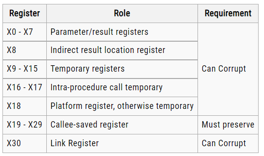
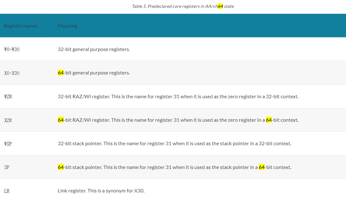
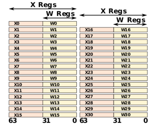
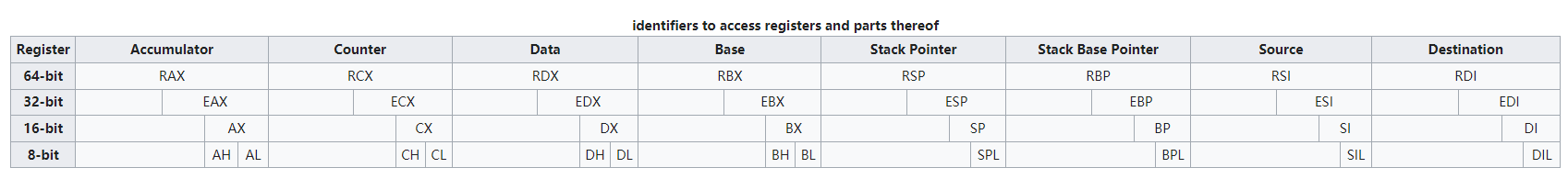
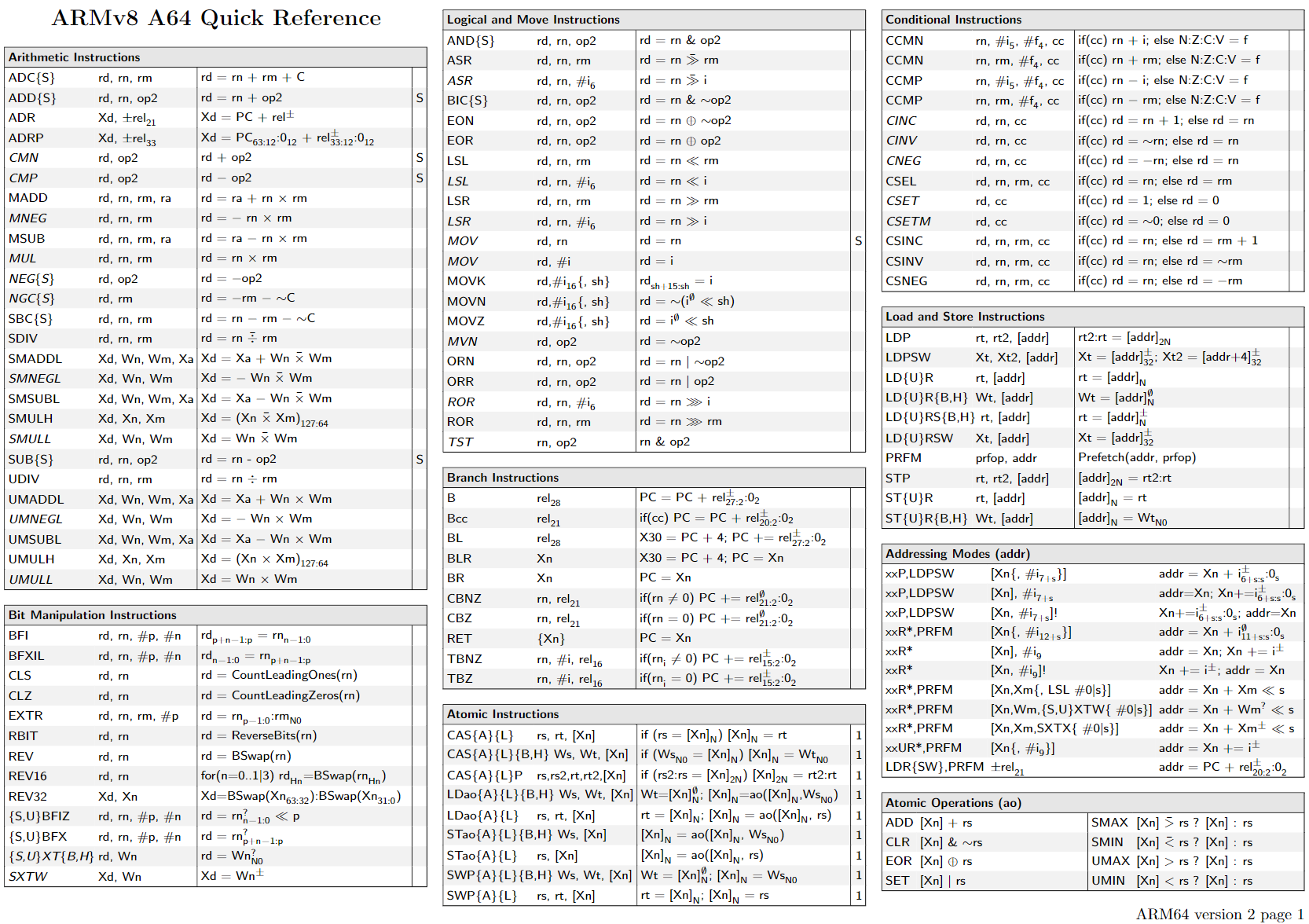
The x86 architecture has 8 General-Purpose Registers (GPR), 6 Segment Registers, 1 Flags Register and an Instruction Pointer. 64-bit x86 has additional registers.

  1. General-Purpose Registers (GPR) - 16-bit naming conventions
    1. Accumulator register (AX). Used in arithmetic operations
    2. Counter register (CX). Used in shift/rotate instructions and loops.
    3. Data register (DX). Used in arithmetic operations and I/O operations.
    4. Base register (BX). Used as a pointer to data (located in segment register DS, when in segmented mode).
    5. Stack Pointer register (SP). Pointer to the top of the stack.
    6. Stack Base Pointer register (BP). Used to point to the base of the stack.
    7. Source Index register (SI). Used as a pointer to a source in stream operations.
    8. Destination Index register (DI). Used as a pointer to a destination in stream operations.
  2. Segment Registers
    1. Stack Segment (SS). Pointer to the stack.
    2. Code Segment (CS). Pointer to the code.
    3. Data Segment (DS). Pointer to the data.
    4. Extra Segment (ES). Pointer to extra data (‘E’ stands for ‘Extra’).
    5. F Segment (FS). Pointer to more extra data (‘F’ comes after ‘E’).
    6. G Segment (GS). Pointer to still more extra data (‘G’ comes after ‘F’).
  3. General-Purpose Registers 64-bit
    1. rax - register a extended
    2. rbx - register b extended
    3. rcx - register c extended
    4. rdx - register d extended
    5. rbp - register base pointer (start of stack)
    6. rsp - register stack pointer (current location in stack, growing downwards)
    7. rsi - register source index (source for data copies)
    8. rdi - register destination index (destination for data copies)

RIP (EIP)

X86-SIMD

http://home.ustc.edu.cn/~shaojiemike/posts/simd/#simd%E5%AF%84%E5%AD%98%E5%99%A8

关于零寄存器

某个寄存器是只读的,存的值一直为0

Most RISC architectures have a “zero register”(WZR/XZR reg31 for ARM) which always reads as zero and cannot be written to.

While the x86/x64 architectures do not have an architectural zero register.

通过zero Idiom :

The register renamer detects certain instructions (xor reg, reg and sub reg, reg and various others) that always zero a register

kunpeng 920

history

2019年1月,华为跟进一步发布自研服务器芯片鲲鹏920。该服务器芯片搭载了64颗海思基于ARMv8架构自研的泰山内核。整体服务器性能较市场现有竞品提升20%。2019年5月,华为宣布获得ARMv8架构永久授权,并且强调华为海思有持续自行开发设计基于ARM授权架构的处理器。

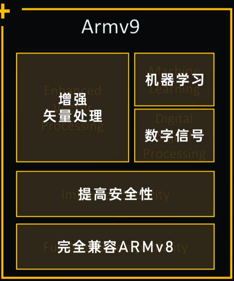
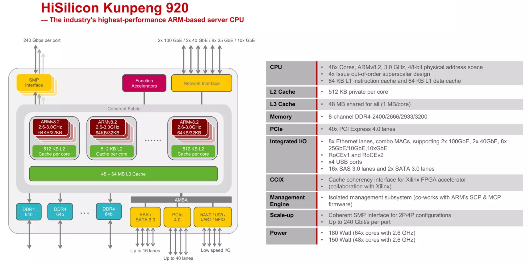
  • AMBA(Advanced Microcontroller Bus Architecture)是ARM公司定义的一个总线架构,用来连接不同的功能模块(如CPU核心、内存控制器、I/O端口等)。AMBA是一种开放标准,用于连接和管理集成在SOC(System on Chip)上的各种组件。它是为了高带宽和低延迟的内部通信而设计的,确保不同组件之间的高效数据传输。
  • ARM的SCP和MCP固件(System Control Processor & Management Control Processor firmware)则是指ARM提供的用于系统控制处理器和管理控制处理器的固件。这些固件通常负责处理系统管理任务,例如电源管理、系统启动和监控、安全性管理等。SCP和MCP是ARM架构中用于系统级管理和控制的专门处理器或子系统。

chip

wikiChip https://en.wikichip.org/wiki/hisilicon/microarchitectures/taishan_v110

1
2
3
4
5
6
7
8
9
10
11
12
13
14
15
16
17
18
19
20
21
22
23
24
25
26
27
28
29
30
31
32
33
34
Architecture:                    aarch64
CPU op-mode(s): 64-bit
Byte Order: Little Endian
CPU(s): 96
On-line CPU(s) list: 0-95
Thread(s) per core: 1
Core(s) per socket: 48
Socket(s): 2
NUMA node(s): 4
Vendor ID: 0x48
Model: 0
Stepping: 0x1
CPU max MHz: 2600.0000
CPU min MHz: 200.0000
BogoMIPS: 200.00
L1d cache: 6 MiB
L1i cache: 6 MiB
L2 cache: 48 MiB
L3 cache: 192 MiB
NUMA node0 CPU(s): 0-23
NUMA node1 CPU(s): 24-47
NUMA node2 CPU(s): 48-71
NUMA node3 CPU(s): 72-95
Vulnerability Itlb multihit: Not affected
Vulnerability L1tf: Not affected
Vulnerability Mds: Not affected
Vulnerability Meltdown: Not affected
Vulnerability Spec store bypass: Not affected
Vulnerability Spectre v1: Mitigation; __user pointer sanitization
Vulnerability Spectre v2: Not affected
Vulnerability Srbds: Not affected
Vulnerability Tsx async abort: Not affected
Flags: fp asimd evtstrm aes pmull sha1 sha2 crc32 atomics fphp asimdhp cpuid asimdrdm j
scvt fcma dcpop asimddp asimdfhm

鲲鹏920明显的几个特点,96个核,4个NUMA node, cache相较于Intel特别大

需要进一步的研究学习

暂无

遇到的问题

暂无

开题缘由、总结、反思、吐槽~~

参考文献

致谢ARM、驭势资本、EETOP…等原编著者,来源华为云社区
https://bbs.huaweicloud.com/blogs/262835

https://developer.arm.com/documentation

RIP register

https://stackoverflow.com/questions/42215105/understanding-rip-register-in-intel-assembly

Assembly Arm

关于X86 与 arm的寄存器的区别写在了arm那篇下

arm

https://developer.arm.com/documentation/dui0068/b/CIHEDHIF

Arm 的四种寻址方式

ldr & str


Aarch64

Arm A64 Instruction Set Architecture
https://modexp.wordpress.com/2018/10/30/arm64-assembly/

直接阅读文档 Arm® A64 Instruction Set Architecture
Armv8, for Armv8-A architecture profile最有效

指令后缀说明

read from ARMv8 Instruction Set Overview 4.2 Instruction Mnemonics

The container is one of:

The subtype is one of:

combine

1
<name>{<subtype>}      <container> 

注意后缀的作用主体

指令速查

官网查找指令: https://developer.arm.com/architectures/instruction-sets/intrinsics


https://armconverter.com/?disasm&code=0786b04e

SIMD/vector

几乎每个指令都可以同时作用在不同寄存器和vector或者scalar上。比如add指令,并没有像X86一样设计vadd或者addps等单独
的指令,如果一定要区分,只能从寄存器是不是vector下手。

根据这个图,确实是有做向量操作的add,FADD是float-add的意思,ADDP是将相邻的寄存器相加放入目的寄存器的意思。不影响是标量scalar还是向量vector的操作。addv是将一个向量寄存器里的每个分量归约求和的意思,确实只能用在向量指令。

由于需要满足64或者128位只有下面几种情况

需要额外注意的是另外一种写法,位操作指令,不在乎寄存器形状shape

1
2
3
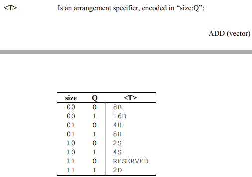
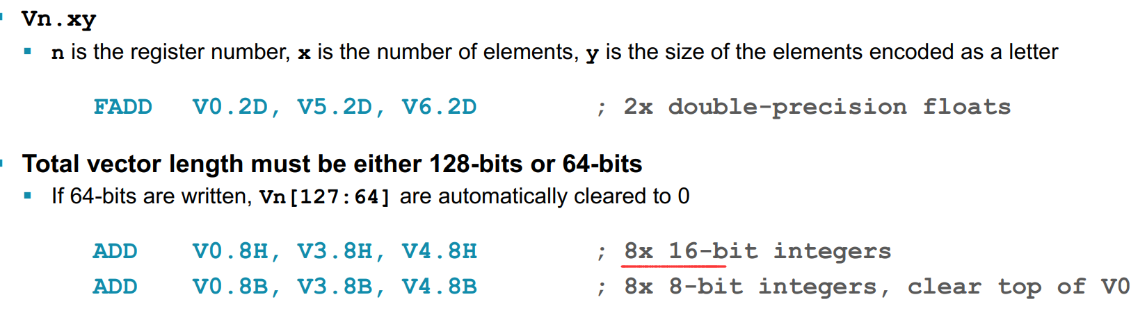
# 128位and
and %q3 %q7 -> %q3
and v3.16b, v3.16b, v7.16b

是同一个意思,但是不支持and v3.8h, v3.8h, v7.8h

1
2
3
DUP //Duplicate general-purpose register to vector.or Duplicate vector element to vector or scalar.
addp //Add Pair of elements (scalar). This instruction adds two vector elements in the source SIMD&FP register and writes
//the scalar result into the destination SIMD&FP register.

calculate

1
2
3
4
5
add
addp //Add Pair of elements (scalar). This instruction adds two vector elements in the source SIMD&FP register and writes the scalar result into the destination SIMD&FP register.
adds // Add , setting flags.
eor // Bitwise Exclusive OR
orr // Move (register) copies the value in a source register to the destination register. Alias of ORR.

Address

1
ADRP // Form PC-relative address to 4KB page.

Branch

1
2
3
4
5
6
7
b.cond // branch condition eg. b.ne
bl //Branch with Link branches to a PC-relative offset, setting the register X30 to PC+4
//带链接的跳转。 首先将当前指令的下一条指令地址保存在LR寄存器,然后跳转的lable。通常用于调用子程序,可通过在子程序的尾部添加mov pc, lr 返回。
blr //Branch with Link to Register calls a subroutine at an address in a register, setting register X30 to PC+4.
cbnz //Compare and Branch on Nonzero compares the value in a register with zero, and conditionally branches to a label at a PC-relative offset if the comparison is not equal. It provides a hint that this is not a subroutine call or return. This instruction does not affect the condition flags.
tbnz // test and branch not zero
ret //Return from subroutine, branches unconditionally to an address in a register, with a hint that this is a subroutine return.

Load/Store

1
2
3
4
5
6
7
8
9
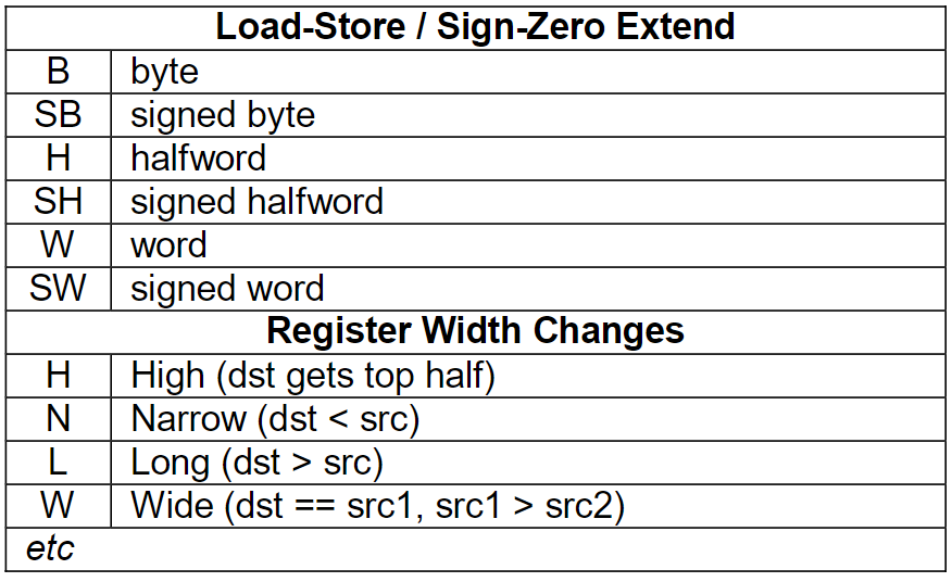
ldrb // b是byte的意思
ldar // LDAR Load-Acquire(申请锁) Register
STLR //Store-Release(释放锁) Register
ldp // load pair(two) register
stp // store pair(two) register
ldr(b/h/sb/sh/sw) // load register , sb/sh/sw is signed byte/half/word
str // store register
ldur // load register (unscaled) unscaled means that in the machine-code, the offset will not be encoded with a scaled offset like ldr uses. or offset is minus.
prfm // prefetch memory

Control/conditional

1
2
3
4
5
6
ccmp // comdition compare
CMEQ // Compare bitwise Equal (vector). This instruction compares each vector element from the frst source SIMD&FP register with the corresponding vector element from the second source SIMD&FP register
CSEL // If the condition is true, Conditional Select writes the value of the frst source register to the destination register. If the condition is false, it writes the value of the second source register to the destination register.
CSINC //Conditional Select Increment returns
CSINV //Conditional Select Invert returns
CSNEG //Conditional Select Negation returns

Logic&Move

1
2
3
4
5
6
7
8
9
10
11
12
13
14
15
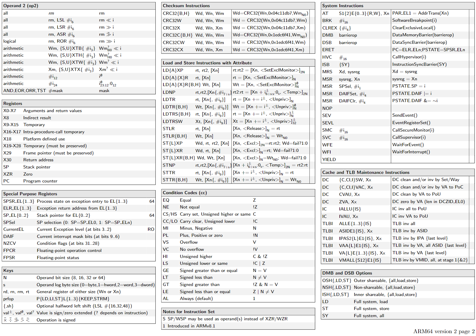
ASRV //Arithmetic Shift Right Variable
lsl //logic shift left
orr //bitwise(逐位) or
eor //Bitwise Exclusive OR
TST/ANDS //Test bits (immediate), setting the condition flags and discarding the result. Alias of ANDS.
MOVZ //Move wide with zero moves an optionally-shifted 16-bit immediate value to a register
UBFM // Unigned Bitfield Move. This instruction is used by the aliases LSL (immediate), LSR (immediate), UBFIZ, UBFX, UXTB, and UXTH
BFM //Bitfield Move
BIC (shifted register) //Bitwise Bit Clear
CLZ // Count Leading Zeros counts the number of binary zero bits before the frst binary one bit in the value of the source register, and writes the result to the destination register.
REV, REV16, REVSH, and RBIT // below
REV //Reverse byte order in a word.
REV16 //Reverse byte order in each halfword independently.
REVSH //Reverse byte order in the bottom halfword, and sign extend to 32 bits.
RBIT //Reverse the bit order in a 32-bit word.

Modifier

1
uxtb // zero extend byte 无符号(Unsigned)扩展一个字节(Byte)到 32位

system

1
2
dmb  //data memory barrier
SVC //The SVC instruction causes an exception. This means that the processor mode changes to Supervisor,

ARM no push/pop

1
2
PUSH {r3}
POP {r3}

are aliases for

1
2
str r3, [sp, #-4]!
ldr r3, [sp], #4

需要进一步的研究学习

暂无

遇到的问题

暂无

开题缘由、总结、反思、吐槽~~

参考文献

https://www.cs.virginia.edu/~evans/cs216/guides/x86.html

https://blog.csdn.net/gaojinshan/article/details/11534569

Intel® Intrinsics Guide

符号说明

_mm_sin_ps intrinsic is a packed 128-bit vector of four 32-bit precision floating point numbers.The intrinsic computes the sine of each of these four numbers and returns the four results in a packed 128-bit vector.

ISA

AVX2 & AVX

AVX2在AVX的基础上完善了256位寄存器的一些实现

FMA

float-point multiply add/sub

include 128/256 bits regs

AVX_VNNI

AVX-VNNI is a VEX-coded variant of the AVX512-VNNI instruction set extension. It provides the same set of operations, but is limited to 256-bit vectors and does not support any additional features of EVEX encoding, such as broadcasting, opmask registers or accessing more than 16 vector registers. This extension allows to support VNNI operations even when full AVX-512 support is not implemented by the processor.

1
2
3
dpbusd  //_mm_dpbusd_avx_epi32
dpwssd // b 与 w 是 byte 和dword。 us和ss是ab两数是不是signed
dpwssds // 最后的s是 signed saturation饱和计算的意思,计算不允许越界。

AVX-512

有时间再看吧

KNC

current generation of Intel Xeon Phi co-processors (codename “Knight’s Corner“, abbreviated KNC) supports 512-bit SIMD instruction set called “Intel® Initial Many Core Instructions” (abbreviated Intel® IMCI).

https://stackoverflow.com/questions/22670205/are-there-simdsse-avx-instructions-in-the-x86-compatible-accelerators-intel

AMX

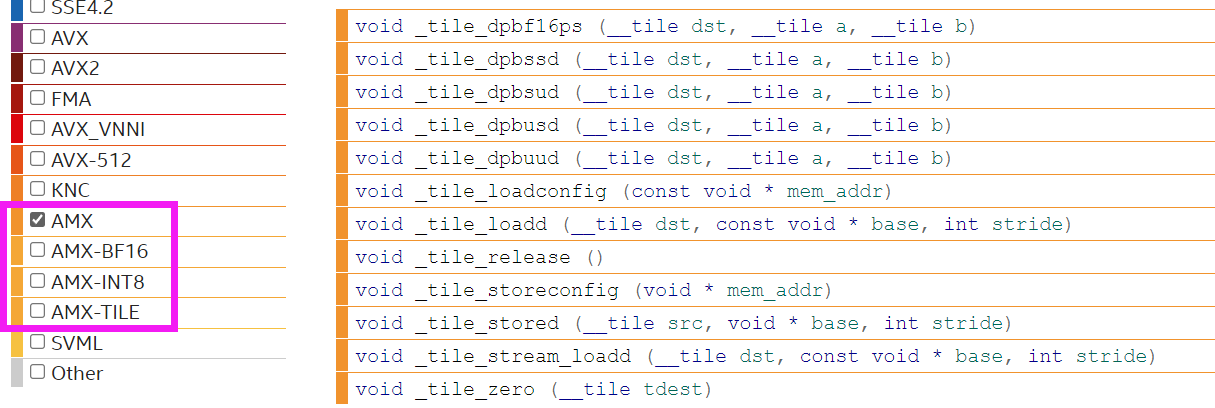
Intel® Advanced Matrix Extensions (Intel® AMX) is a new 64-bit programming paradigm consisting of two components:

  • A set of 2-dimensional registers (tiles) representing sub-arrays from a larger 2-dimensional memory image
  • An accelerator that is able to operate on tiles; the first implementation of this accelerator is called TMUL (tile matrix multiply unit).

这个不适用于特殊矩阵和稀疏矩阵,这类一般先转换化简再SIMD

SVML

Short Vector Math Library Operations (SVML)

The Intel® oneAPI DPC++/C++ Compiler provides short vector math library (SVML) intrinsics to compute vector math functions. These intrinsics are available for IA-32 and Intel® 64 architectures running on supported operating systems. The prototypes for the SVML intrinsics are available in the immintrin.h file.

Using SVML intrinsics is faster than repeatedly calling the scalar math functions. However, the intrinsics differ from the scalar functions in accuracy.

需要进一步的研究学习

暂无

遇到的问题

暂无

开题缘由、总结、反思、吐槽~~

参考文献

Manual AVX256 SIMD

类型区别

The __m256 data type can hold eight 32-bit floating-point values.

The __m256d data type can hold four 64-bit double precision floating-point values.

The __m256i data type can hold thirty-two 8-bit, sixteen 16-bit, eight 32-bit, or four 64-bit integer values

向量预取

1
_mm512_mask_prefetch_i32extgather_ps

Load & Store

1
2
3
4
5
6
7
8
__m256i _mm256_loadu_epi32 (void const* mem_addr) //读入连续的256位数据,为32位int
_mm256_lddqu_si256 //上面识别不了也可以考虑这个
__m256d _mm256_loadu_pd (double const * mem_addr) // 读入连续4个double
__m256d _mm256_broadcast_sd (double const * mem_addr) // 读取一个double,并复制4份
__m256d _mm256_i64gather_pd (double const* base_addr, __m256i vindex, const int scale) // 间隔读取
scatter // 类似间隔读取
_mm512_mask_prefetch_i32extgather_ps // 有选择预取
mask // 根据掩码选择不读,0等操作
1
2
_mm256_stream_pd // 跳过cache直接写入内存,但是需要对齐
_mm_storeu_si128 // int直接写入内存,不需要对齐

不连续读取

1
2
3
long long int vindexList = [0,2,4,6];
__m256i vindex = __mm256_loadu_epi64(vindexList);
__m256d vj1 = __mm256_i64gather_pd(&rebuiltCoord[jj*k], vindex, 1);

设置每个元素

1
2
__m256d _mm256_set_pd (double e3, double e2, double e1, double e0) // 设置为四个元素
__m256d _mm256_set1_pd (double a) // 设置为同一个元素

Arithmetic

1
2
3
4
_mm256_hadd_epi16 // Horizontally add eg.dst[15:0] := a[31:16] + a[15:0]
_mm256_mulhi_epi16 // Multiply the packed signed 16-bit integers in a and b, producing intermediate 32-bit integers, and store the high 16 bits of the intermediate integers in dst.
_mm256_sign_epi16 // 根据b的值,将-a/0/a存入dst
// 乘加,乘减,的计算组合也有

横向结果归约

1
_mm256_reduce_add_ph // 求和

手动实现向量浮点abs绝对值

1
2
3
static const double DP_SIGN_One = 0x7fffffffffffffff;
__m256d vDP_SIGN_Mask = _mm256_set1_pd(DP_SIGN_One);
vj1 = _mm256_and_pd(vj1, vDP_SIGN_Mask);

Shift

1
2
_mm_bsrli_si128 // byte shift right 
_mm_slli_epi16 // shift left

logic

1
2
_mm_test_all_zeros
_mm_test_all_ones //判断是不是全0或1

Elementary Math Functions

向量化 取反、sqrt

Convert

1
_mm256_cvtepi32_pd // Convert_Int32_To_FP64

Compare

1
_mm256_cmp_pd // 按照double 32 bit 比较

Swizzle(混合)

1
2
3
4
5
_mm256_blendv_pd // 根据mask结果,从a和b里选择写入dst
_mm_blend_epi32 // 寄存器内数据的移动
_mm256_permute4x64_epi64 // 寄存器高位复制到低位
VEXTRACTF128 __m128d _mm256_extractf128_pd (__m256d a, int offset); // 寄存器内数据的移动
VUNPCKHPD __m512d _mm512_unpackhi_pd( __m512d a, __m512d b); //寄存器内数据的移动

类型转换

1
2
__m256d _mm256_undefined_pd (void)
__m128i low = _mm256_castsi256_si128(v); //__m256i 变 type __m128i,源向量较低的128位不变地传递给结果。这种内在的特性不会向生成的代码引入额外的操作。

1
2
3
4
5
6
7
8
9
10
11
12
13
14
15
16
Select4(SRC, control) {
CASE (control[1:0]) OF
0: TMP ←SRC[31:0];
1: TMP ←SRC[63:32];
2: TMP ←SRC[95:64];
3: TMP ←SRC[127:96];
ESAC;
RETURN TMP
}

VSHUFPS (VEX.128 encoded version) 
DEST[31:0] ←Select4(SRC1[127:0], imm8[1:0]);
DEST[63:32] ←Select4(SRC1[127:0], imm8[3:2]);
DEST[95:64] ←Select4(SRC2[127:0], imm8[5:4]);
DEST[127:96]←Select4(SRC2[127:0], imm8[7:6]);
DEST[MAXVL-1:128] ←0


之后float类型转换为double,再求和。

需要进一步的研究学习

暂无

遇到的问题

暂无

开题缘由、总结、反思、吐槽~~

参考文献

https://www.intel.com/content/www/us/en/docs/intrinsics-guide/index.html#text=_mm256_loadu_pd&ig_expand=4317