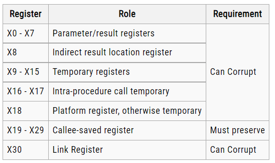
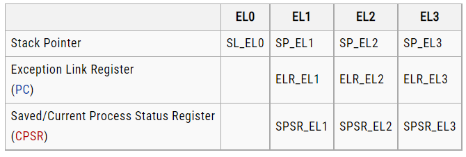
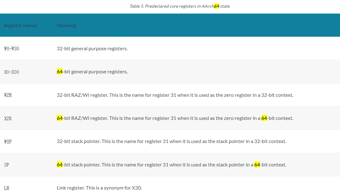
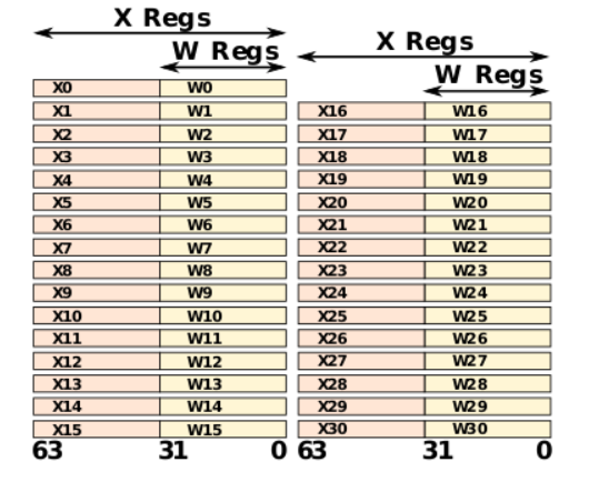
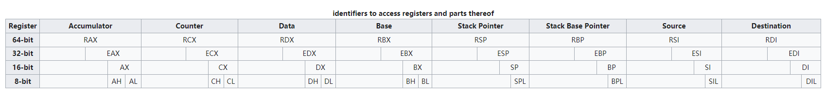
关于X86 与 arm的寄存器的区别写在了arm那篇下
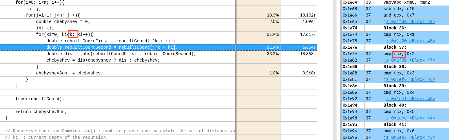
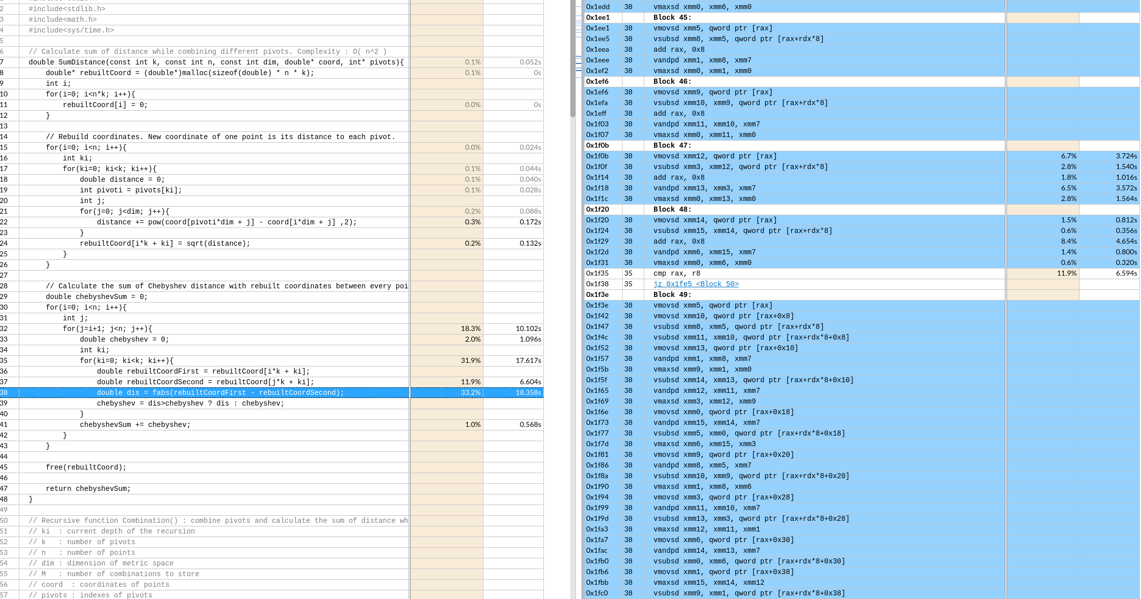
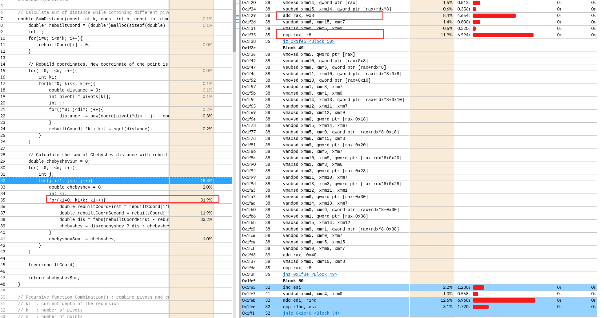
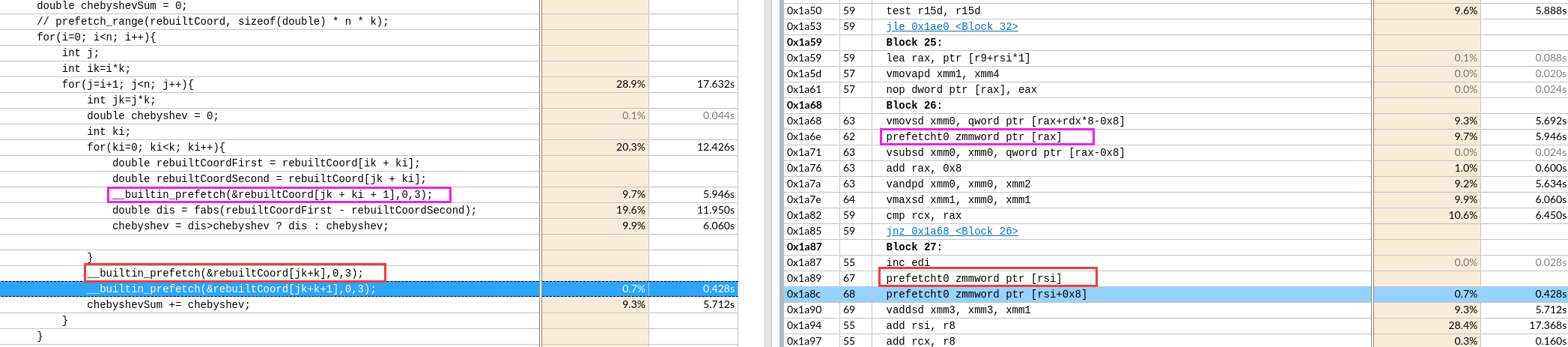
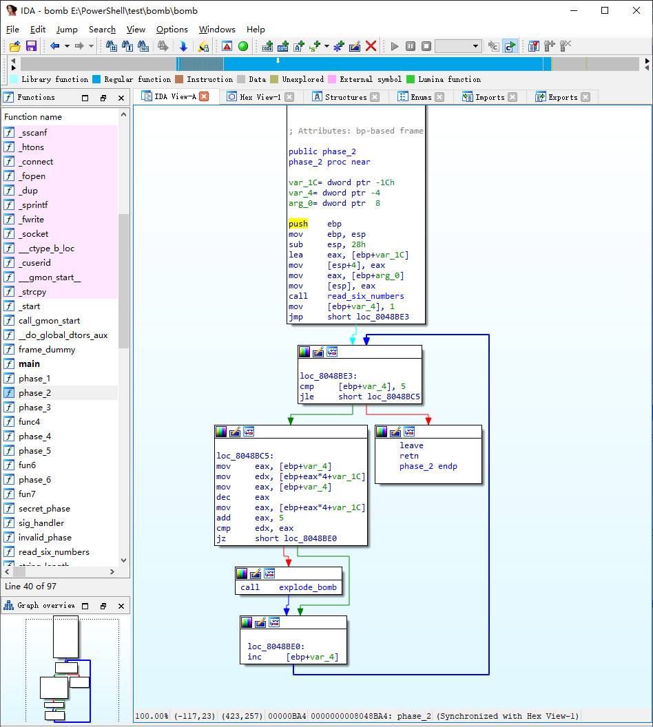
IDA analysis
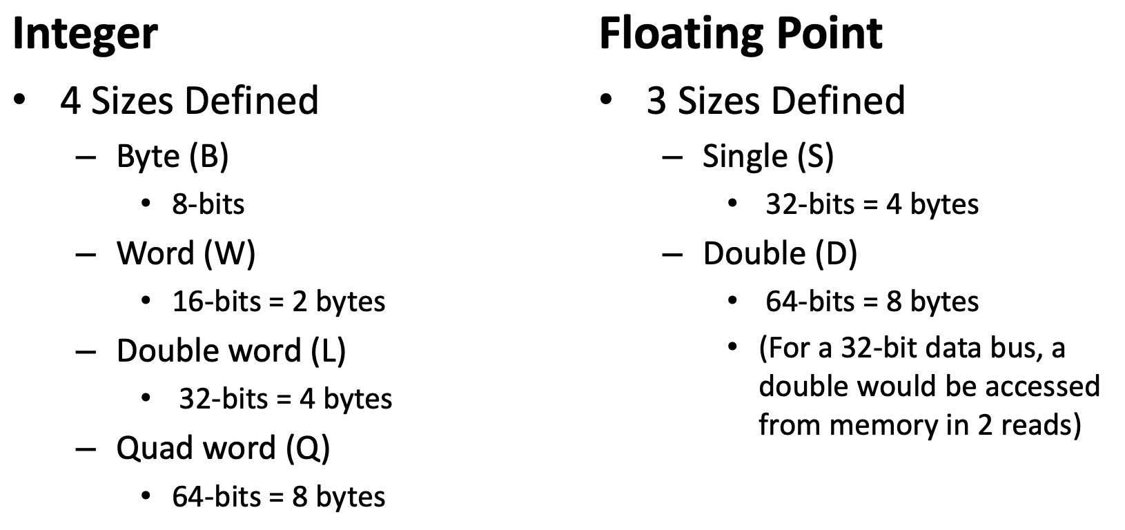
word/ dword/ qword
In x86 terminology/documentation, a “word” is 16 bits
x86 word = 2 bytes
x86 dword = 4 bytes (double word)
x86 qword = 8 bytes (quad word)
x86 double-quad or xmmword = 16 bytes, e.g. movdqa xmm0, [rdi].
常见X86汇编
https://en.wikipedia.org/wiki/X86_instruction_listings
https://www.felixcloutier.com/x86/
https://officedaytime.com/simd512e/
1 | SHR # Shift right (unsigned shift right) |
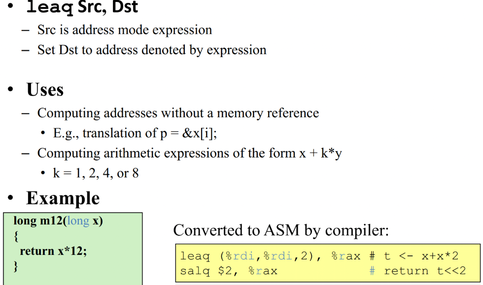
lea & leaq
1 | lea -0xc(%ebp),%eax |
1 | // x is %rdi, result is %rax 就是计算地址,没有寻址操作 |
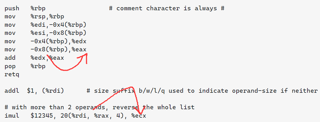
call & ret
Call 地址:返回地址入栈(等价于“Push %eip,mov 地址,%eip”;注意eip指向下一条尚未执行的指令)ret:从栈中弹出地址,并跳到那个地址(pop %eip)
leave
leave:使栈做好返回准备,等价于
1 | mov %ebp,%esp |
compare order
1 | cmpl $0x5,$0x1 |
X86 load store
X86 不像 ARM有专门的ldr, str指令。是通过mov实现的
movswl (%rdi), %eax sign-extending load from word (w) to dword (l). Intel movsx eax, word [rdi]
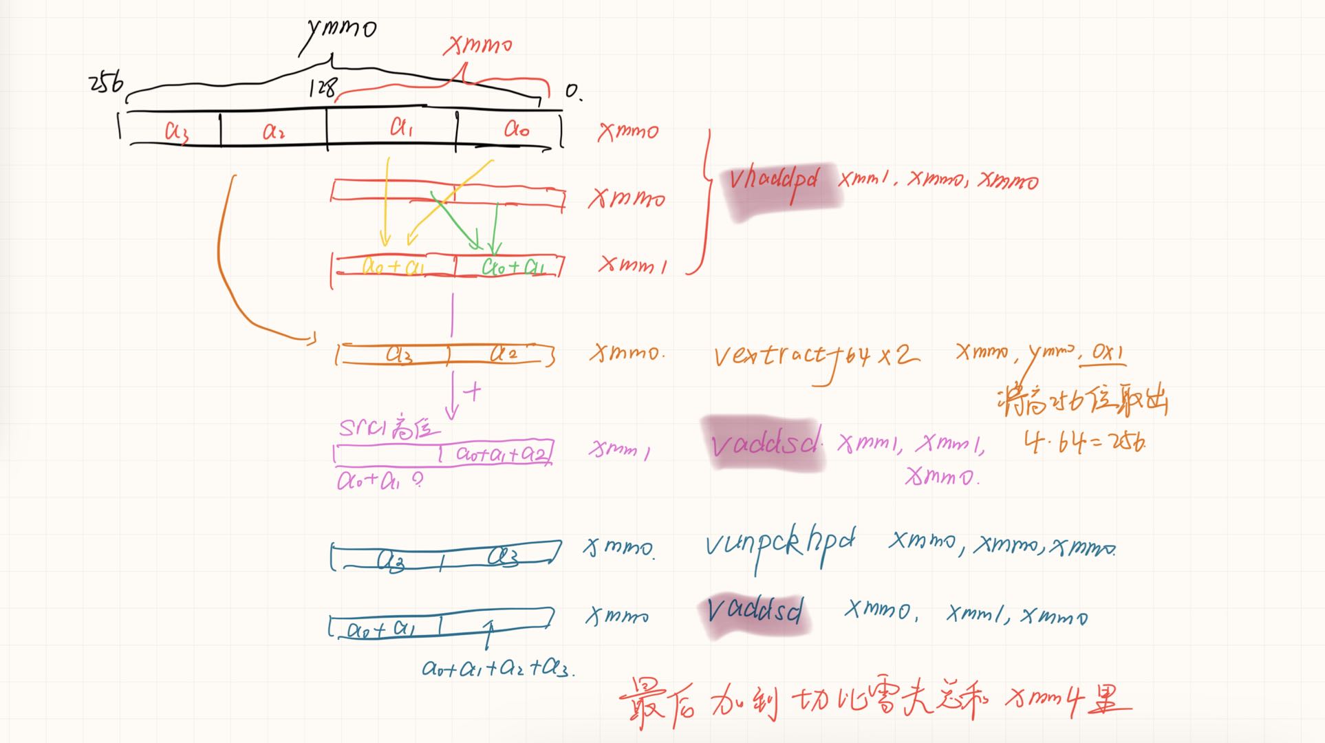
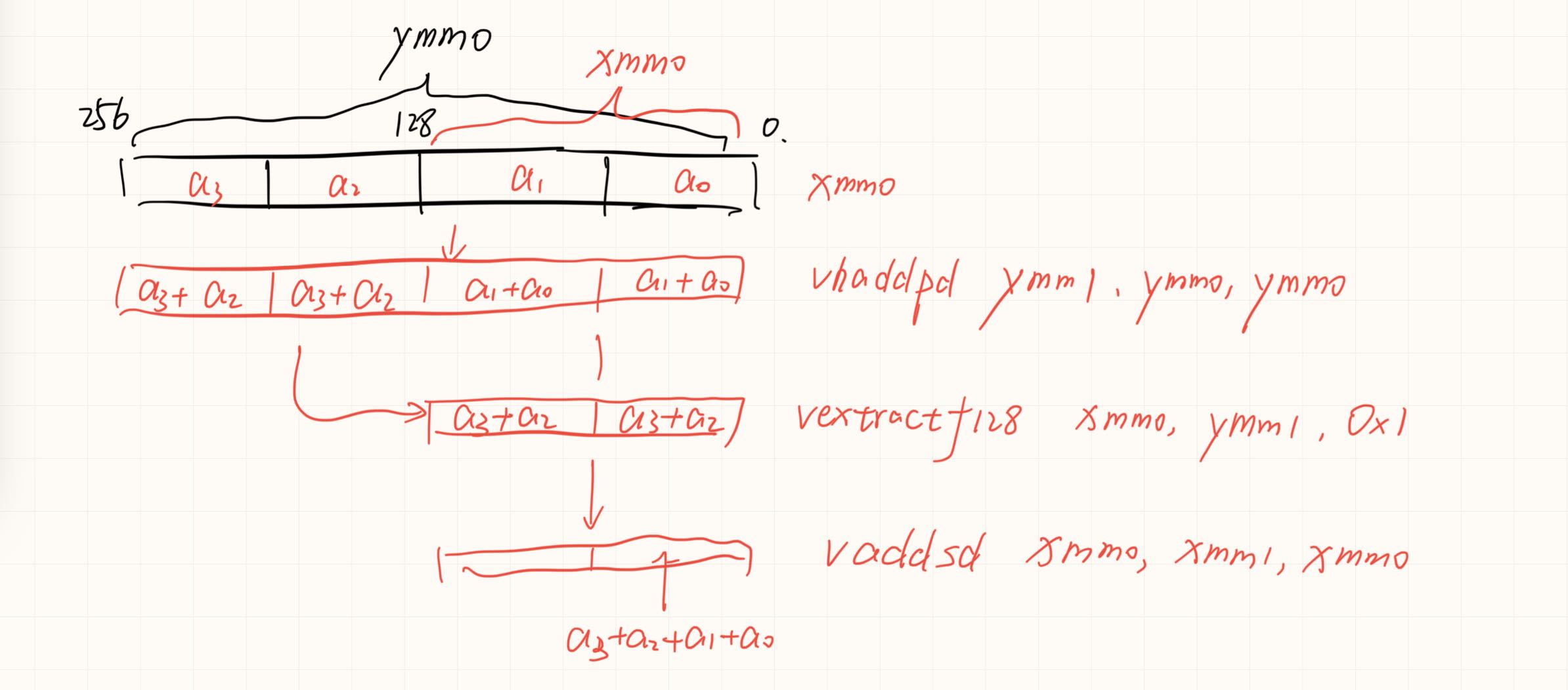
AVX
https://docs.oracle.com/cd/E36784_01/html/E36859/gntbd.html
1 | vxorpd XORPD |
test & jump
1 | test al, al |
The test instruction performs a logical and of the two operands and sets the CPU flags register according to the result (which is not stored anywhere). If al is zero, the anded result is zero and that sets the Z flag. If al is nonzero, it clears the Z flag. (Other flags, such as Carry, oVerflow, Sign, Parity, etc. are affected too, but this code has no instruction testing them.)
The jne instruction alters EIP if the Z flag is not set. There is another mnemonic for the same operation called jnz.
1 | test %eax,%eax |
注意 cmp不等于 test
The TEST operation sets the flags CF and OF to zero.
The SF is set to the MSB(most significant bit) of the result of the AND.
If the result of the AND is 0, the ZF is set to 1, otherwise set to 0.
kinds of jump
AT&T syntax jmpq *0x402390(,%rax,8) into INTEL-syntax: jmp [RAX*8 + 0x402390].
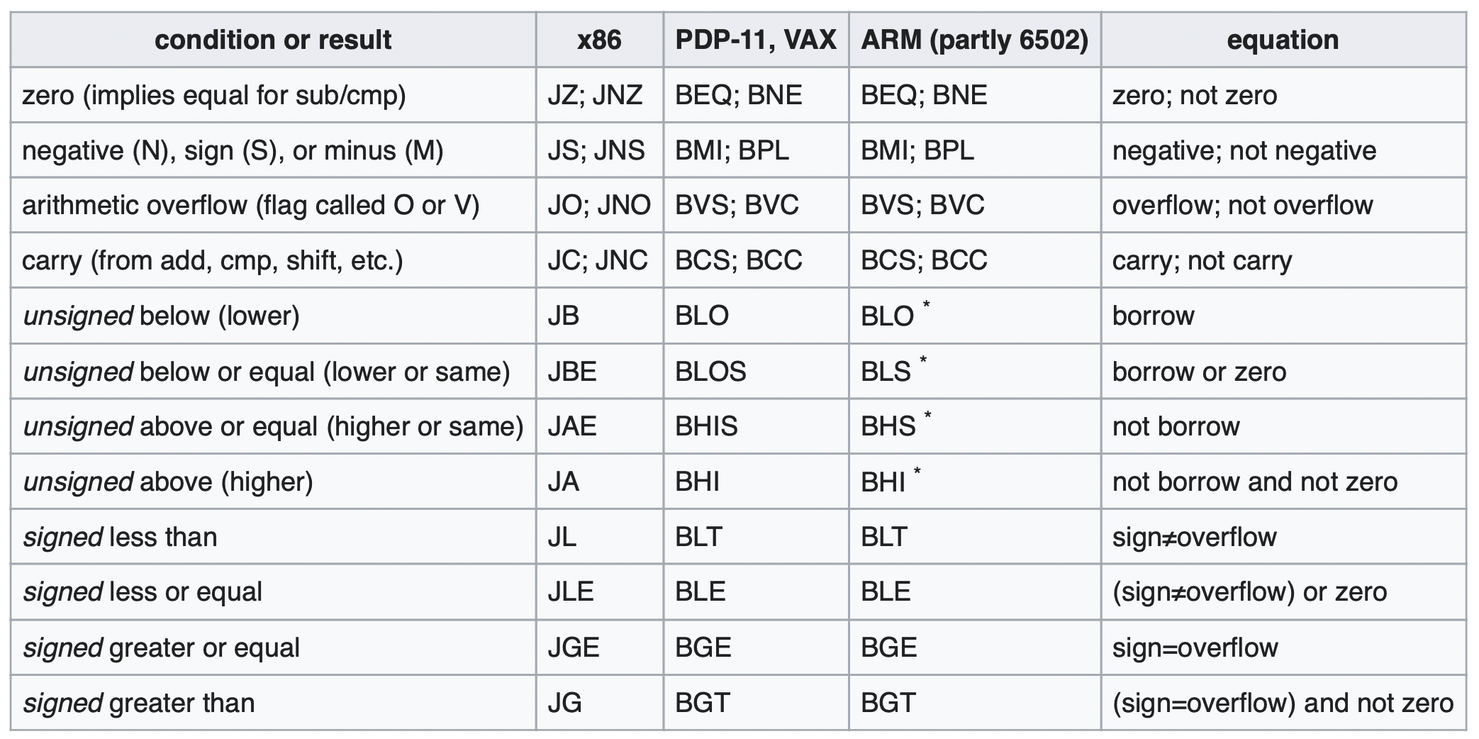
ja VS jg
JUMP IF ABOVE AND JUMP IF GREATER
ja jumps if CF = 0 and ZF = 0 (unsigned Above: no carry and not equal)
jg jumps if SF = OF and ZF = 0 (signed Greater, excluding equal)
FLAGS
cmp performs a sub (but does not keep the result).
cmp eax, ebx
Let’s do the same by hand:
1 | reg hex value binary value |
The flags are set as follows:
1 | OF (overflow) : did bit 31 change -> no |
Carry Flag
Carry Flag is a flag set when:
a) two unsigned numbers were added and the result is larger than “capacity” of register where it is saved.
Ex: we wanna add two 8 bit numbers and save result in 8 bit register. In your example: 255 + 9 = 264 which is more that 8 bit register can store. So the value “8” will be saved there (264 & 255 = 8) and CF flag will be set.
b) two unsigned numbers were subtracted and we subtracted the bigger one from the smaller one.
Ex: 1-2 will give you 255 in result and CF flag will be set.
Auxiliary Flag is used as CF but when working with BCD. So AF will be set when we have overflow or underflow on in BCD calculations. For example: considering 8 bit ALU unit, Auxiliary flag is set when there is carry from 3rd bit to 4th bit i.e. carry from lower nibble to higher nibble. (Wiki link)
Overflow Flag is used as CF but when we work on signed numbers.
Ex we wanna add two 8 bit signed numbers: 127 + 2. the result is 129 but it is too much for 8bit signed number, so OF will be set.
Similar when the result is too small like -128 - 1 = -129 which is out of scope for 8 bit signed numbers.
register signed & unsigned
Positive or negative
The CPU does not know (or care) whether a number is positive or negative. The only person who knows is you. If you test SF and OF, then you treat the number as signed. If you only test CF then you treat the number as unsigned.
In order to help you the processor keeps track of all flags at once. You decide which flags to test and by doing so, you decide how to interpret the numbers.
register multiply
The computer makes use of binary multiplication(AND), followed by bit shift (in the direction in which the multiplication proceeds), followed by binary addition(OR).
1 | 1100100 |
for more:
How computer multiplies 2 numbers?
And:
Binary multiplier - Wikipedia
Memory and Addressing Modes
声明静态代码区域
DB, DW, and DD can be used to declare one, two, and four byte data locations,
1 | # 基本例子 |
数组的声明,The DUP directive tells the assembler to duplicate an expression a given number of times. For example, 4 DUP(2) is equivalent to 2, 2, 2, 2.
1 |
|
寻址
32位X86机器寻址支持
- 最多支持32位寄存器和32位有符号常数相加
- 其中一个寄存器可以再乘上 2,4,8
1 | # right |
指定存储在地址的数据大小
1 | mov BYTE PTR [ebx], 2 ; Move 2 into the single byte at the address stored in EBX. |
汇编寄存器顺序,作用方向
这和汇编器语法有关:
X86 instructions
For instructions with two operands, the first (lefthand) operand is the source operand, and the second (righthand) operand is the destination operand (that is, source->destination).
1 | mov eax, ebx — copy the value in ebx into eax |
AT&T syntax
AT&T Syntax is an assembly syntax used in UNIX environments, that originates from AT&T Bell Labs. It is descended from the MIPS assembly syntax. (AT&T, American Telephone & Telegraph)
AT&T Syntax is an assembly syntax used mostly in UNIX environments or by tools like gcc that originated in that environment.
语法特点:https://stackoverflow.com/tags/att/info
需要注意的:
- Operands are in destination-last order
- Register names are prefixed with
%, and immediates are prefixed with$sub $24, %rspreserves 24 bytes on the stack.
- Operand-size is indicated with a
b/w/l/qsuffix on the mnemonicaddb $1, byte_table(%rdi)increment a byte in a static table.- The mov suffix (b, w, l, or q) indicates how many bytes are being copied (1, 2, 4, or 8 respectively)
imul $13, 16(%rdi, %rcx, 4), %eax32-bit load fromrdi + rcx<<2 + 16, multiply that by 13, put the result in%eax. Intelimul eax, [16 + rdi + rcx*4], 13.movswl (%rdi), %eaxsign-extending load from word (w) to dword (l). Intelmovsx eax, word [rdi].
Intel syntax (used in Intel/AMD manuals).
The Intel assembler(icc,icpc我猜) uses the opposite order (destination<-source) for operands.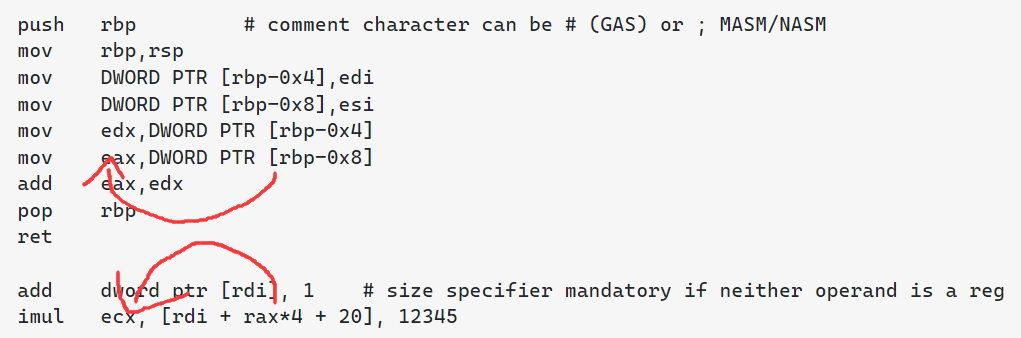
语法特点: https://stackoverflow.com/tags/intel-syntax/info
RISC-V
1 | beq rs1, rs2, Label #RISC-V |
反汇编器
但是这个语法不是很重要,因为decompiler有选项控制语法
objdump has -Mintel flag, gdb has set disassembly-flavor intel option.
gcc -masm=intel -S or objdump -drwC -Mintel.
需要进一步的研究学习
暂无
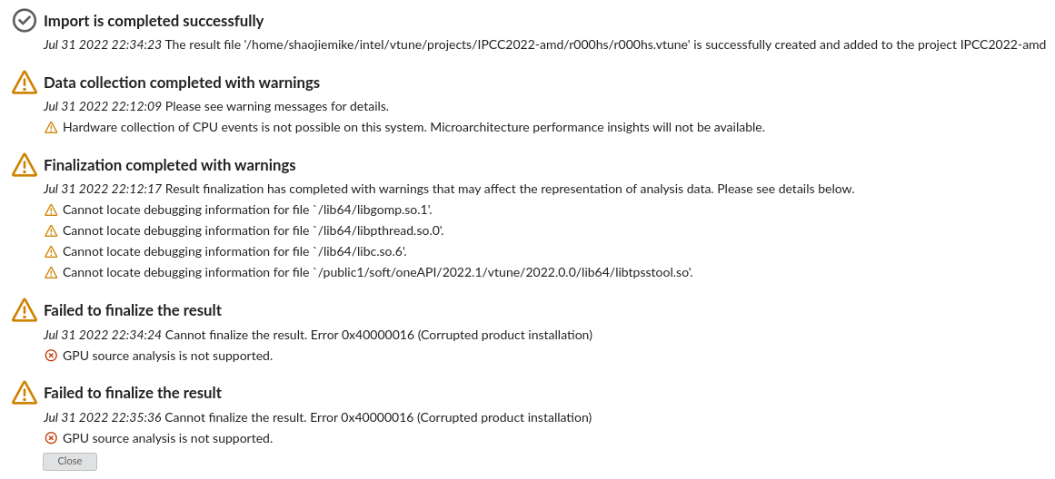
遇到的问题
暂无